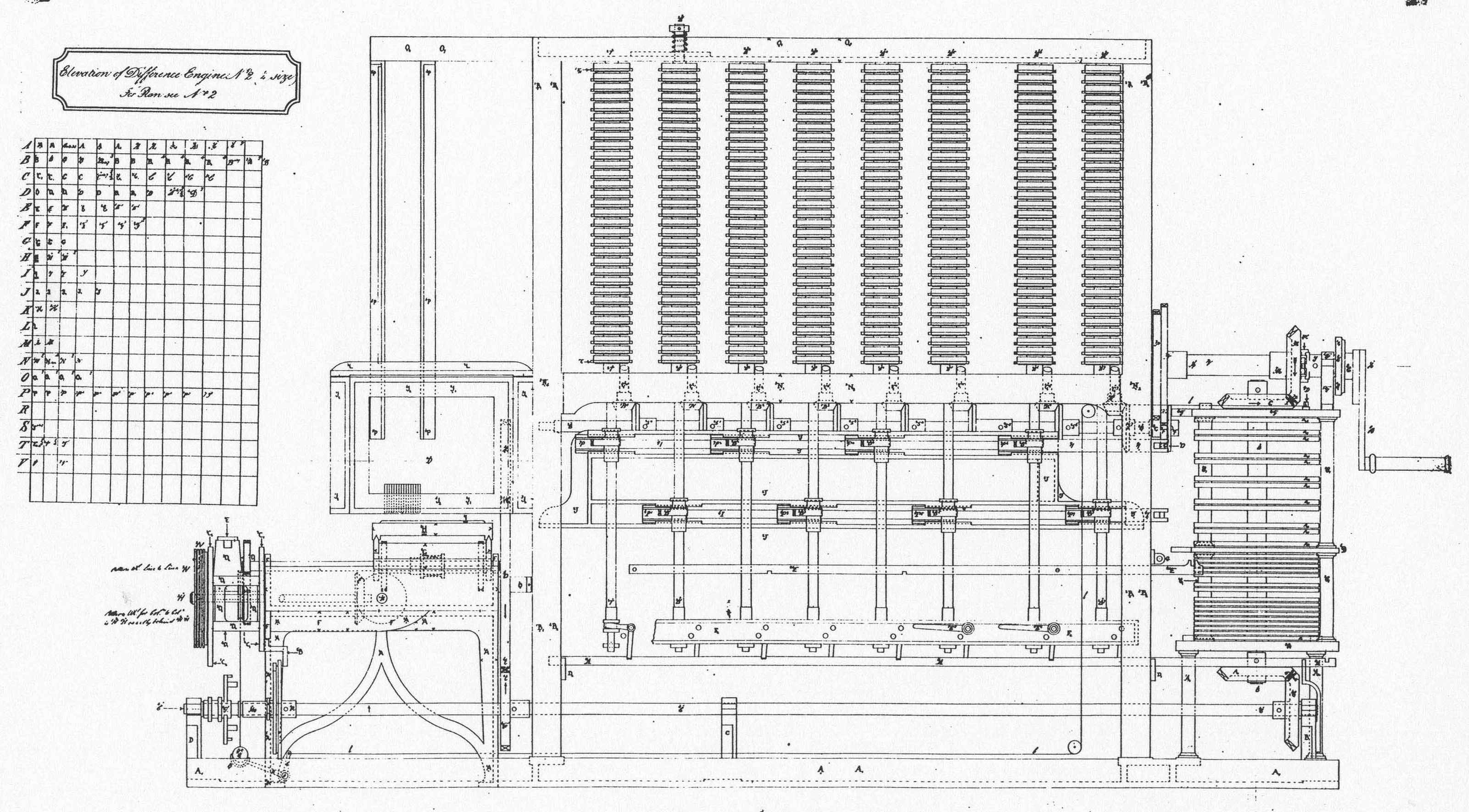
To show that a computer's architecture is 'independent' of the technology used to implement it i've made the Difference Engine 9000, the DE9000, the great, great, great, grandfather of HAL9000. This hard-coded 'computer' is implemented in a Field Programmable Gate Array (FPGA), defined using a Hardware Description Language (HDL), in this case my language of preference VHDL. The original Difference Engine is shown in figure 1, numbers are stored as signed 31 decimal digit values, one number per column, allowing the machine to store eight (very big) numbers. For more information on this machine refer to: (Link) (Link).
Figure 1 : Difference Engine
Babbage was commissioned by the British government to provide accurate Log, Trig and other mathematical tables for naval navigation. Work on his Difference Engine No. 1 (DE1) was started in 1822, funding was later withdrawn due to increasing costs. He redesigned this machine during 1847 - 1849, producing Difference Engine No. 2 (DE2). However, Babbage only completed partial prototypes, he did not produce a fully working machine (it was later completed by the British Science museum). DE2 evaluated polynomials using the method of finite differences, e.g. to calculate the values of y = x^3. To do this you would manually calculate the first five values, taking the repeated difference of these values as shown in the top table of figure 2. This produces a set of initial coefficients i.e. 0, 1, 6, 6, and 0. Then using only addition functions these coefficients can be used to generate other values of x^3, as shown in the bottom table of figure 2.
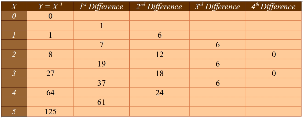
Figure 2 : Method of Differences, coefficients calculation (top), table generation (bottom)
In general a computer's architecture is independent of the technology used to implement it, however, there may be practical limitations associated with particular technologies e.g. size, cost, power etc, that make one technology preferable to another. The simplified architectural block diagram for DE2 is shown in figure 3, comprising of eight adders and eight registers. Note, an adder + memory is often referred to as an accumulator (ACC). I don't think my new version is quite the same as the original, i think that had only seven adders. However, with a few small changes this hardware can be implemented in silicon i.e. the new and improved, DE9000.

Figure 3 : Simplified architecture
To implement this architecture's hardware a Field Programmable Gate Array (FPGA) will be used i.e. user configurable hardware. For more information on FPGA devices refer to: (Link). To define this architecture's hardware units, VHDL descriptions (text) will be used. VHDL is a double acronym: V standing for very high speed integrated circuit (VHSIC), HDL for hardware description language. This language was commissioned by the American Department of Defence in the early 1980's as an implementation independent method of describing electronic systems, especially hardware. For more information on the VHDL language refer to: (Link). The DE9000 hardware is defined in a number of text files as shown in figure 4.
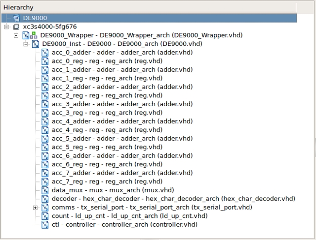
Figure 4 : VHDL file hierarchy
FPGAs are binary devices using Boolean logic gates to construct the desired functional units, therefore, the 31 decimal digit numbers need to be represented in base 2. This will require 103 or 104 bit values (depending if the stated 31 digits included the sign digit or not) :
VALUE = 09999999999999999999999999999999
2^101 = 02535301200456458802993406410752
2^102 = 05070602400912917605986812821504
2^103 = 10141204801825835211973625643008
2^104 = 20282409603651670423947251286016
2^105 = 40564819207303340847894502572032
Note, could of used Binary Coded Decimal (BCD) to make the hardware a little more comparable to the original, will have a go later, but this will require slightly more hardware. Like the original DE2, this new implementation only performs the algorithm of the method of finite differences. Initial coefficient values are passed through generic parameters when the VHDL component is instantiated. To configure a FPGA these text files are synthesized into a configuration bit file that defines the required internal FPGA connections to realise the DE9000 architecture in silicon. The DE9000 component is instantiated within a GENERATE loop. This allows one or more difference engines to be 'built' within the FPGA, each initialised with different coefficients, all working in parallel, transmitting their results over multiple serial links.
Figure 4 : VHDL
The RTL schematic (circuit diagram) of the DE9000 is shown in figure 5, the eight repeated accumulator (ACC) units can be seen in the top row of the schematic, the serial transmitter and controller are in the bottom right. Using this FPGA there is more than enough space for multiple difference engines to be implemented on the same FPGA. This is can be easily implemented by changing the constant MAX in the generate loop. After a bit of trial and error 28 difference engines can fit in this FPGA, as shown in figures 6 and 7. However, the main limitation is the FPGA board used (figure 8), as it only has two serial port interfaces i.e. IO bound rather than processing.
Figure 5 : Schematic
Figure 6 : Floorplan for DE9000, starting top left 1,2,4,8,16,20,24 and 28
Figure 7 : FPGA resources for 1 - 28 DE9000
To display the result of the output register instead of a printing press an RS232 serial port interface has been added to this design. This converts the output register's 104bit result into a hexadecimal ASCII representation that can be transmitted to a PC. For more information on this interface refer to: (Link) (Link). Using a terminal program running on a PC the data values generated by this computing machine can be displayed to the user as shown in figure 9. These data values are displayed as 32 digit hexadecimal values i.e. base 16.
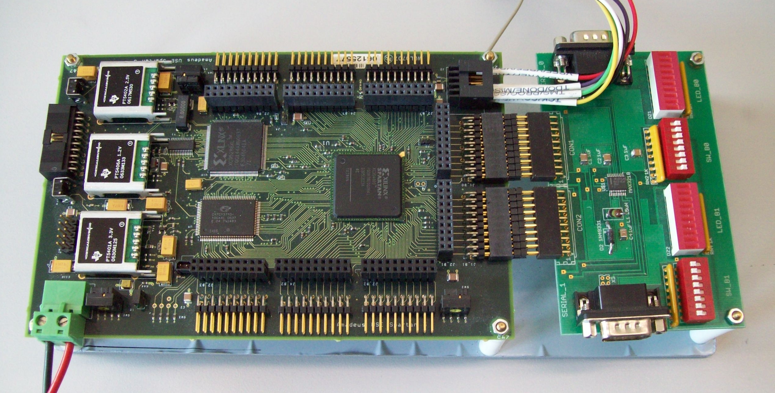
Figure 8 : FPGA board
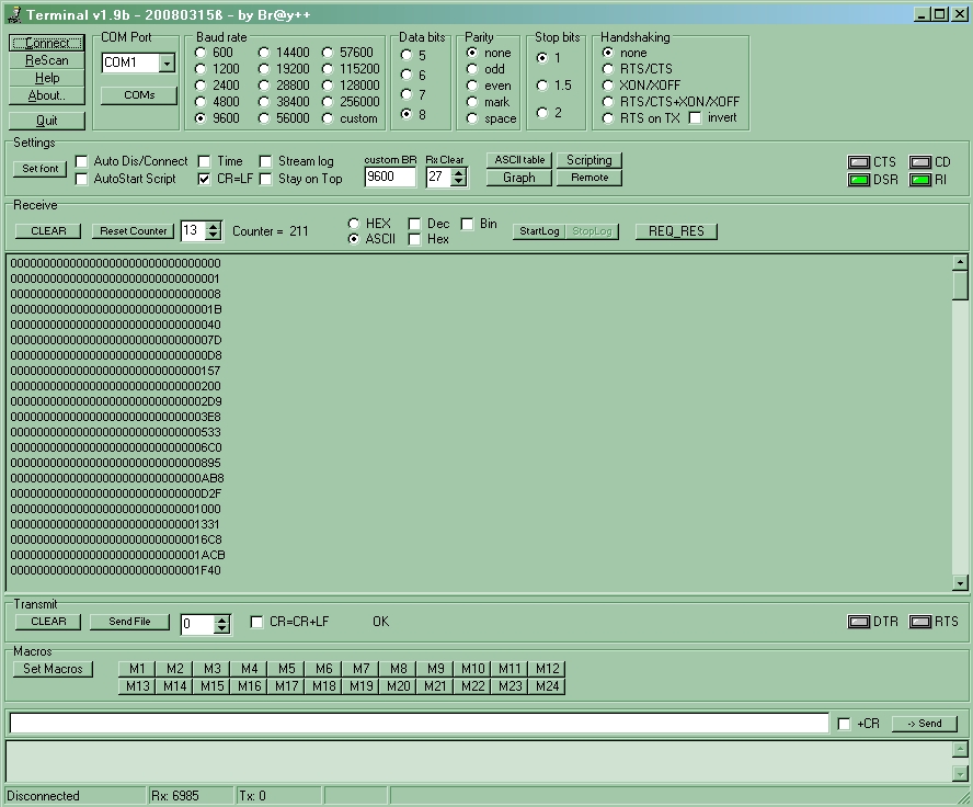
Figure 9 : Terminal display
Converting these hexadecimal values into decimal values, we can see that this hardware has regenerated the y = x^3 values as defined in figure 2.
000000 = 0
000001 = 1
000008 = 8
00001B = 27
000040 = 64
00007D = 125
0000D8 = 216
000157 = 343
000200 = 512
0002D9 = 729
0003E8 = 1000
...
Why were the binary numbers converted into base 16 and not base 10, simple, binary-to-hexadecimal conversion is easy in hardware, binary-to-decimal is quite tricky in hardware. Will perhaps add this functionality later i.e. for ease of viewing. The complete VHDL description for DE9000 can be downloaded here: (Link).

This work is licensed under a Creative Commons Attribution-NonCommercial-NoDerivatives 4.0 International License.
Contact email: mike@simplecpudesign.com