I've always used simple switching logic to help explain how Boolean logic gates function and how they are implemented. If you take a step back and look at the evolution of computers from first to fourth generation, a lot has changed, but if you consider the operation of the different technologies defining these generations you can still boil their functionality down to very simple on/off switches e.g. CMOS logic gates. To me this is a nice starting point, if you understand the basics everything builds upon these ideas, block by block, until you end up with computer. A key motivation here is that if you don't understand the limitations of the technology used you will not understand why a computer's architecture looks the way it does. Therefore, to start this journey i built some basic logic gates out of relays. I like relays as you can actually see the switches working/moving, which i think makes a more interesting demo, well that's what the electronics engineer in me thinks :).
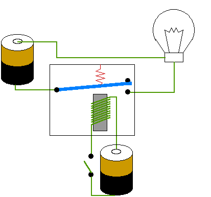
A relay can be thought of as a simple voltage controlled switch. Most people have done a bit of physics at some time and have played with magnets, wrapped some wire around a nail, connected the coil to a battery to make an electromagnet, this is basically what a relay is, we simple add some switch contacts that the electromagnetic can either pulls closed or pushes open, making or breaking a circuit. When the electromagnet is de-energised i.e. the voltage removed, the force holding the switch contacts together (or apart) is removed, a spring returning the contacts to their resting state, as shown in figure 1. In this example when a voltage is applied to the coil the electromagnet pulls together the switch contacts, completing the circuit, allowing current to flow through the bulb i.e. we are using a voltage to switch on or off another voltage. At first glance you may think why is this useful i.e. if i want to control the bulb why don't i simply switch power to the bulb directly, why bother to use a switch to control another switch, well thats where switch logic comes in. If you would like more information on relays refer to (Link).
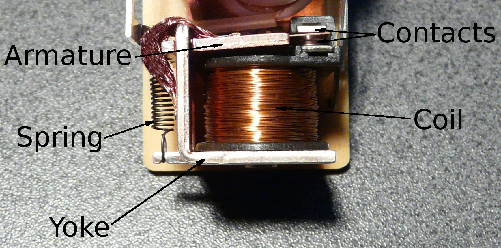
Figure 1 : Relay (src)
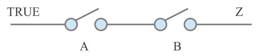
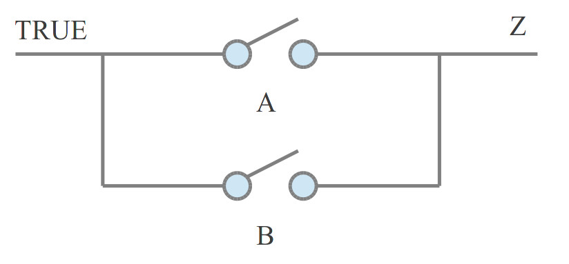
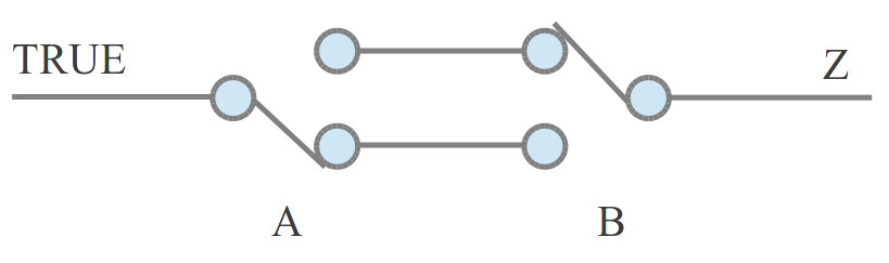
I was first introduced to switch or ladder logic (Link) when working offshore (gas/oil industry). You find a lot of the older programmable logic controllers used in industrial applications (Link). These were "programmed" using this graphical representation i.e. a network of switches connected in series or parallel to implement the system's desired behaviour. To illustrate this consider the AND gate. In its simplest form this can be implemented using two switches connected in series as shown in figure 2. For a logic TRUE to be connected to output Z, switches A and B must be closed, thus implementing the desired AND function. To represent TRUE and FALSE we will use different voltages. When people traditional think of Boolean logic circuits a TRUE (logic 1) is represented as +5V and a FALSE (logic 0) is represented as a 0V. However, this is not a hard and fast rule, we could reverse this, we could use 0V to represent a TRUE and +5V to represented a FALSE. We just need to assign two different voltages, representing the two different Boolean states. In the relay circuits we will be looking at i have used +12V to represent TRUE and open-circuit (not connected to anything, disconnected) to represent FALSE. Note, how we encode these logical states is normally determined by the technology used, for the case of the relays they use +12V to energise their cores, therefore, it simplifies construction to use +12V to represent a logical state.
| A | B | Z |
|---|---|---|
| FALSE | FALSE | FALSE |
| FALSE | TRUE | FALSE |
| TRUE | FALSE | FALSE |
| TRUE | TRUE | TRUE |
Figure 2 : AND gate
To realise this switch circuit using relays the circuit shown in figure 3 can be used. Here two relays K1 and K2 are used to implement switches A and B. Note, the schematic in figure 3 isn't quite correct the relays are simple single-pole single-through (SPST) relays, rather than the single-pole double-through (SPDT) ones shown in the circuit diagram. The reason for this mismatch was that there was an existing PCB component package of a similar size, i didn't have to redraw. If the terms SPST and SPDT don't make any sense refer here for more information on switches (Link). For more information on the relays used their datasheet is available here: (Link). From a current view point these are very over spec-ed, but i went with these large relays so you could easily see the switch contacts moving etc.
When +12V is applied to terminal B relay K1 is energised closing contacts K1. If input A is connected to 0V or disconnected relay K2 will not be energised, therefore, +12V (VCC) will not be connected to output Z. Only when both terminal A and B are connected to +12V will the output Z be driven to +12V i.e. both switches will be closed. In addition to the relays i also included some snubbing diodes D1 and D2 to remove high voltage spikes generated when the coils are de-energised, also some LEDs on the inputs and outputs so that you can see the state of each signal.
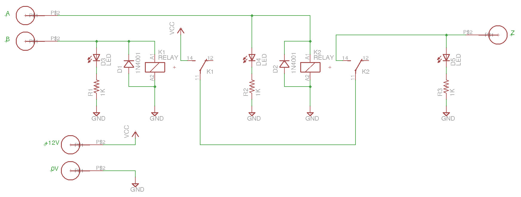
Figure 3 : AND gate relay circuit
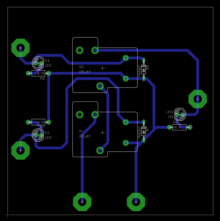
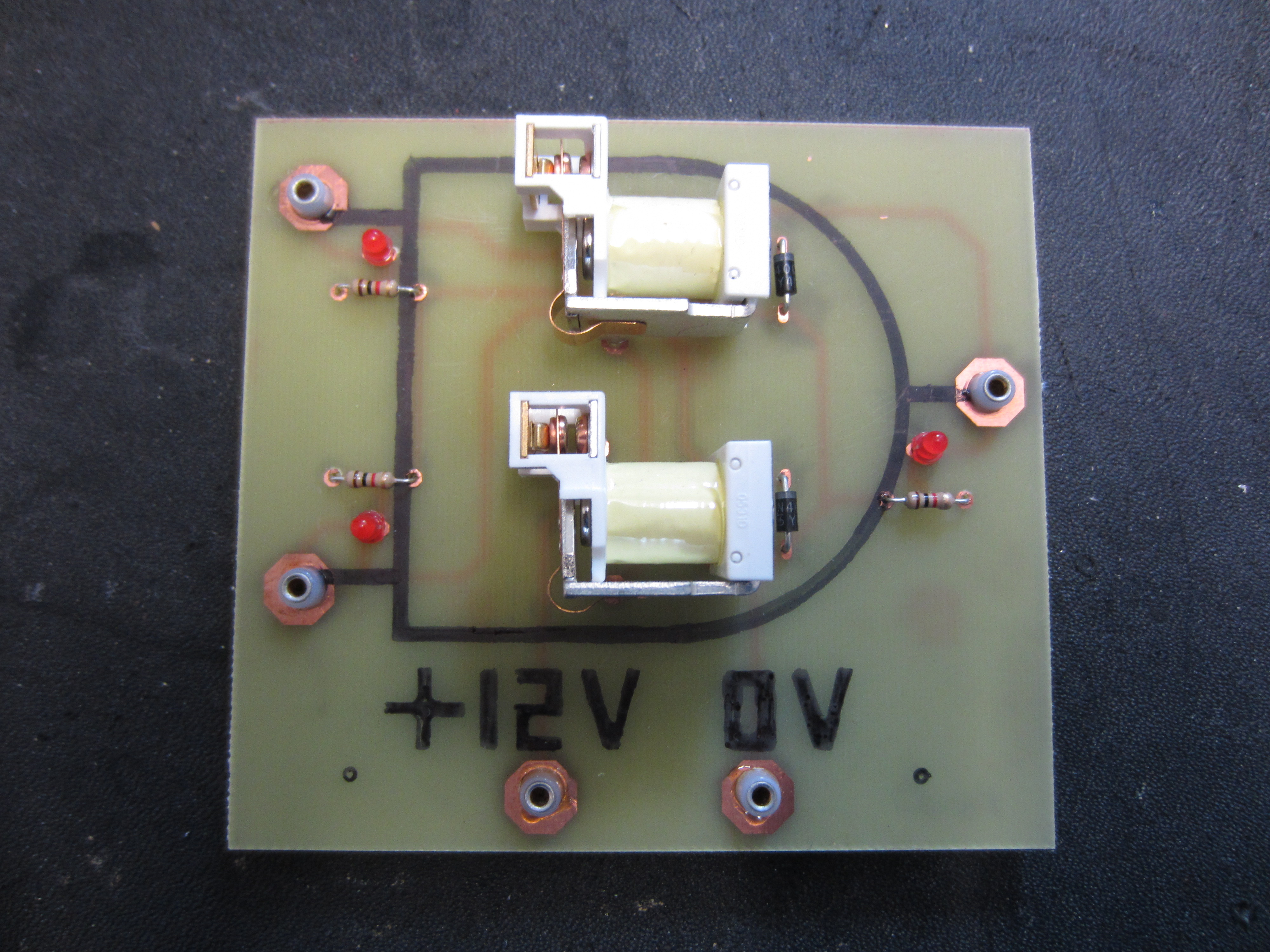
Figure 4 : AND gate relay PCB
Very similar to the AND gate, but the switches are now in parallel rather than being in series. If either relay controlling switch A or B is energised a path is formed from the TRUE signal to the output Z, thus implementing the desired logic OR function. The circuit diagram and PCB used to implement this logic gate are shown in figures 6 and 7.
| A | B | Z |
|---|---|---|
| FALSE | FALSE | FALSE |
| FALSE | TRUE | TRUE |
| TRUE | FALSE | TRUE |
| TRUE | TRUE | TRUE |
Figure 5 : OR gate
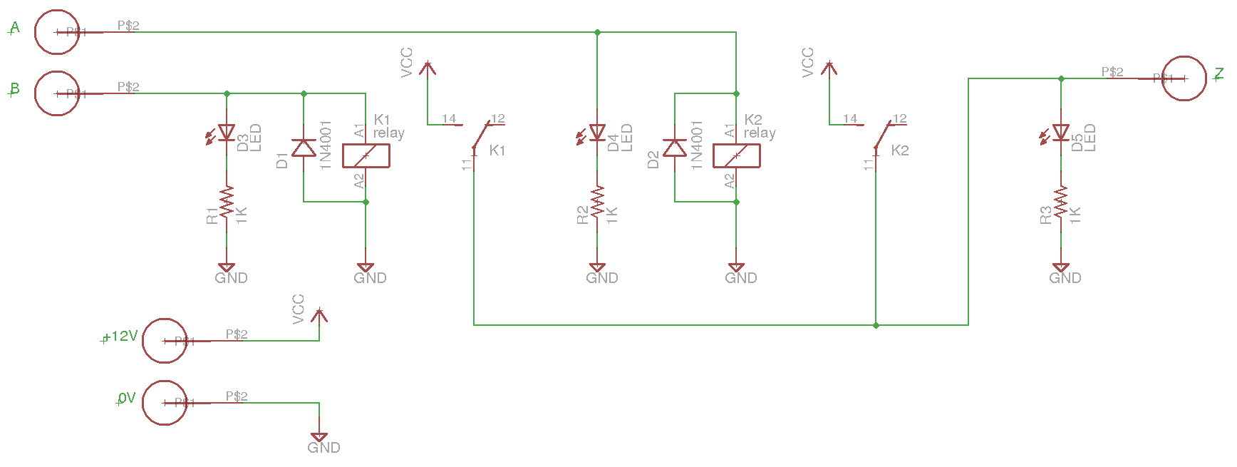
Figure 6 : OR gate relay circuit
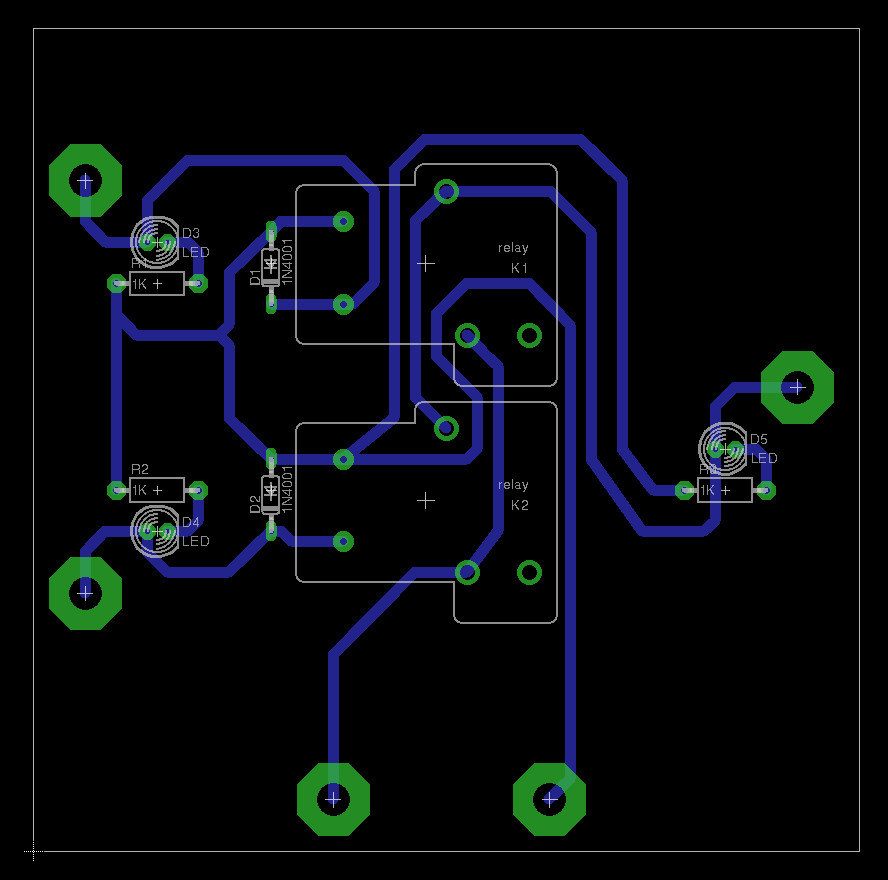
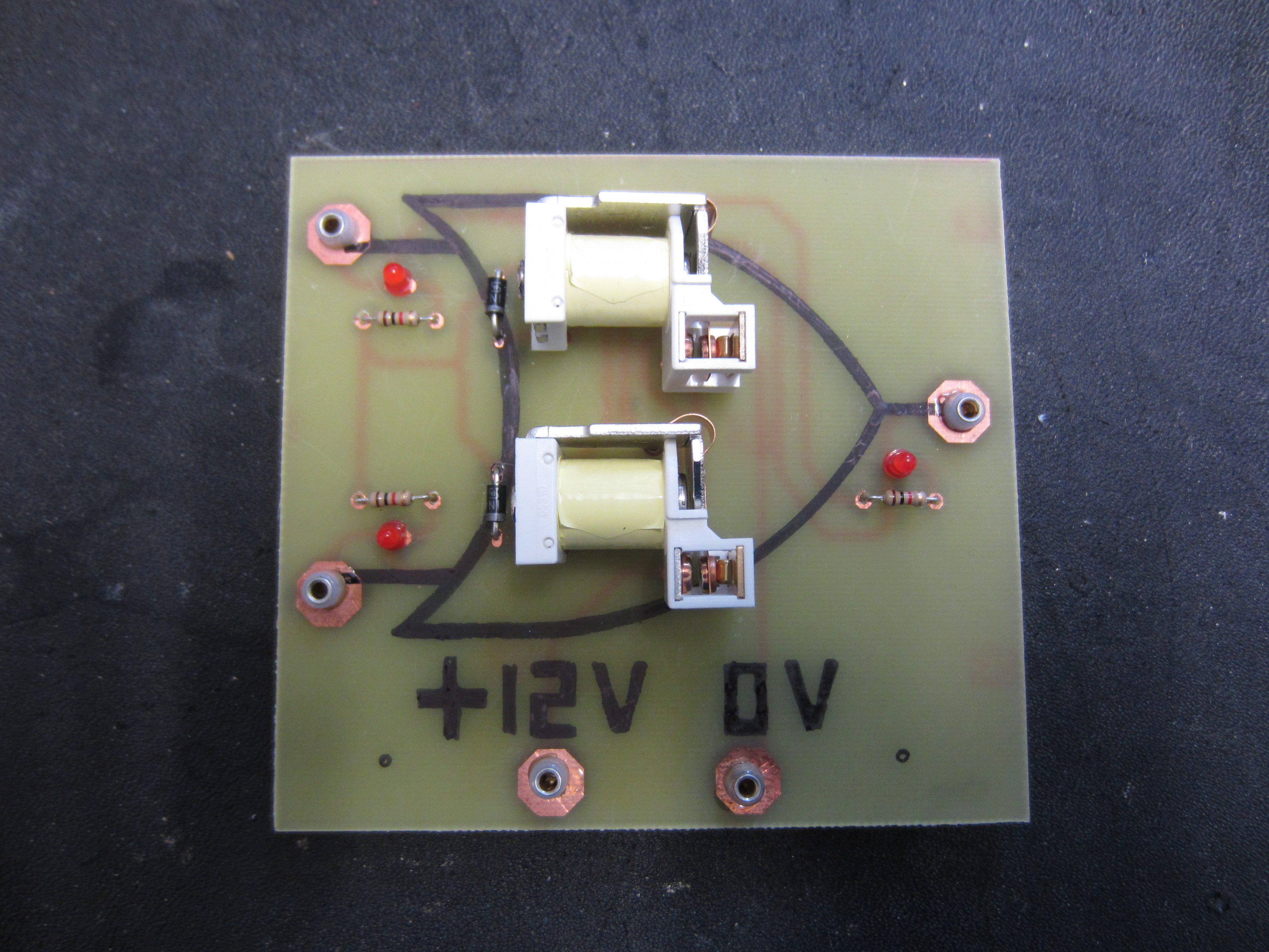
Figure 7 : OR gate relay PCB
A slightly more complex gate, but can still be implemented using two relays, but we do need to use a slightly more complex relay i.e. a SPDT, with an extra contact as shown in figure 8. The SPST relays used in the AND and OR gates close a single contact when the relay is energised. The SPDT relays used in the XOR gate (Link), both make and break electrical contacts each time it is energised or de-energised. Figure 8 shows the position of switches A and B when both switches (relays) are de-energised i.e. off. In this state there is no path form the TRUE signal to the output. If either relay controlling switch A or B is energised one switch contact is moved to its opposite position forming a link from the TRUE signal to the output. If both relays are energised then this link is again broken. The circuit diagram and PCB used to implement this logic gate are shown in figures 9 and 10.
| A | B | Z |
|---|---|---|
| FALSE | FALSE | FALSE |
| FALSE | TRUE | TRUE |
| TRUE | FALSE | TRUE |
| TRUE | TRUE | FALSE |
Figure 8 : XOR gate
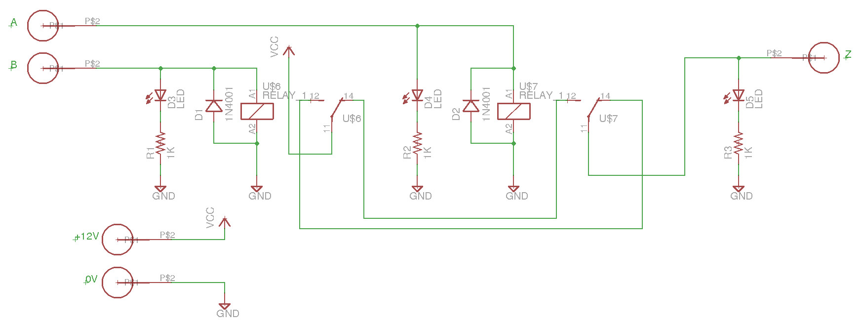
Figure 9 : XOR gate relay circuit
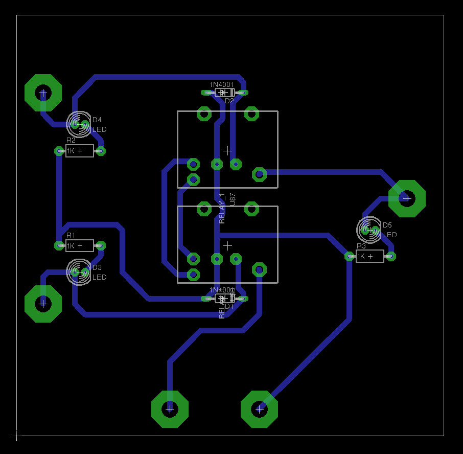
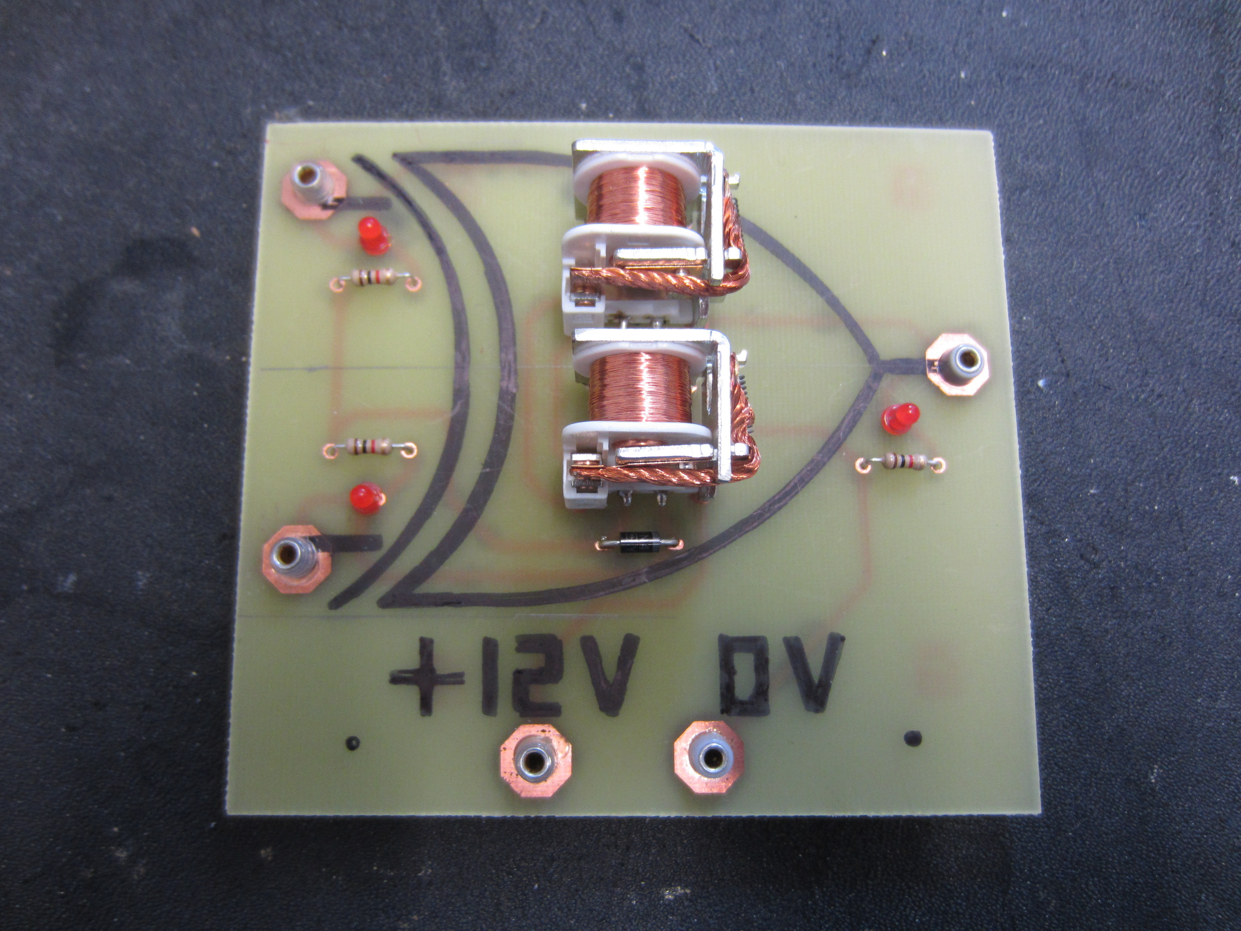
Figure 10 : XOR gate relay PCB
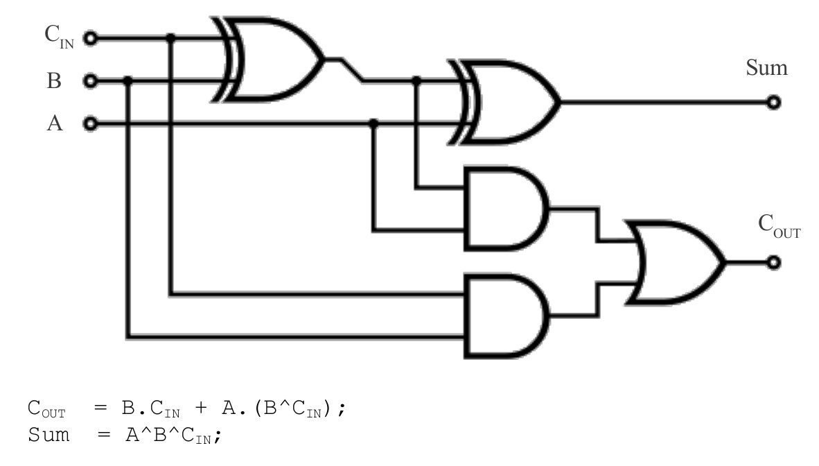
So at this point we have three logic gates: AND, OR and XOR, this allows you to make any logical function, as we can use the XOR gate to make a NOT gate or a BUFFER. Therefore, its time to put these together to implement a circuit that does something useful e.g. adds binary digits. Adders are one of the key building blocks of any computer. Note, i always find this one interesting, Boolean logic works on TRUE and FALSE, a positional number system working in base-2 works on 0 and 1 i.e. integers, numbers. TRUE and FALSE are not the same data type and 0 and 1, but we move freely from one to the other, a TRUE is a 1, a FALSE is a 0, not always stopping to consider the difference. Anyway, your classic full adder is constructed using the logic circuit shown in figure 11.
| A | B | Cin | Sum | Cout |
|---|---|---|---|---|
| 0 | 0 | 0 | 0 | 0 |
| 0 | 0 | 1 | 1 | 0 |
| 0 | 1 | 0 | 1 | 0 |
| 0 | 1 | 1 | 0 | 1 | 1 | 0 | 0 | 1 | 0 |
| 1 | 0 | 1 | 0 | 1 |
| 1 | 1 | 0 | 0 | 1 |
| 1 | 1 | 1 | 1 | 1 |
Figure 11 : Full Adder circuit diagram
Made a plywood base to hold it all together, as shown in figure 12. Note, this circuit is implemented from two half adders (AND + XOR), that each perform the addition of two bits. The OR combining each CARRY into the final CARRY_OUT. You can also spot in figure 12 a couple of extra boards, made a switch board to allow me to enter the three input bits: A, B and Cin. Also made an output LED board to display the SUM (bottom) and CARRY_OUT (top) state. Finally a DC power board to connect the 2.1mm power connector to the 2mm plugs used to wire this circuit. A short video of the circuit in action is available here: (Link).
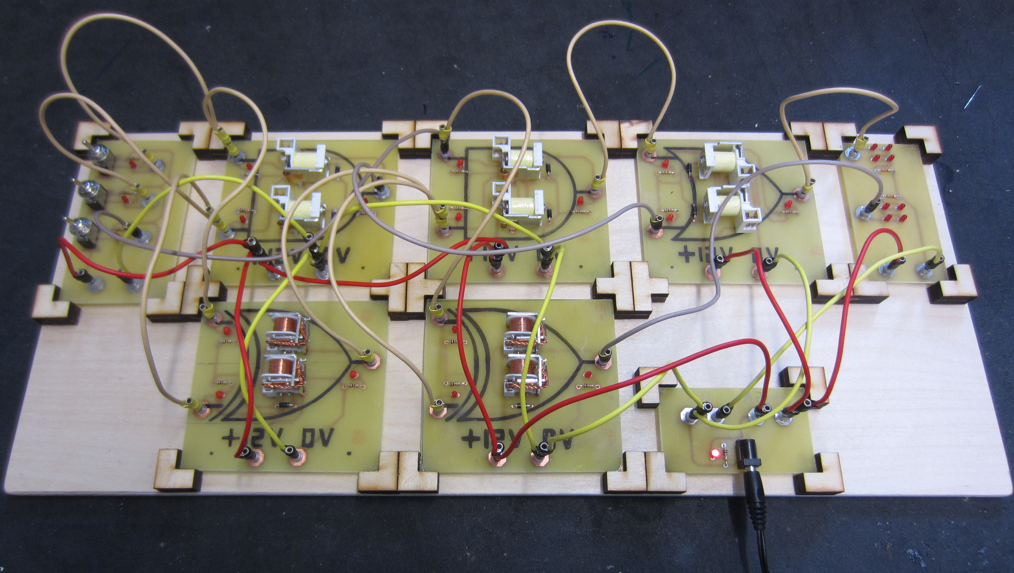
Figure 12 : Full Adder circuit
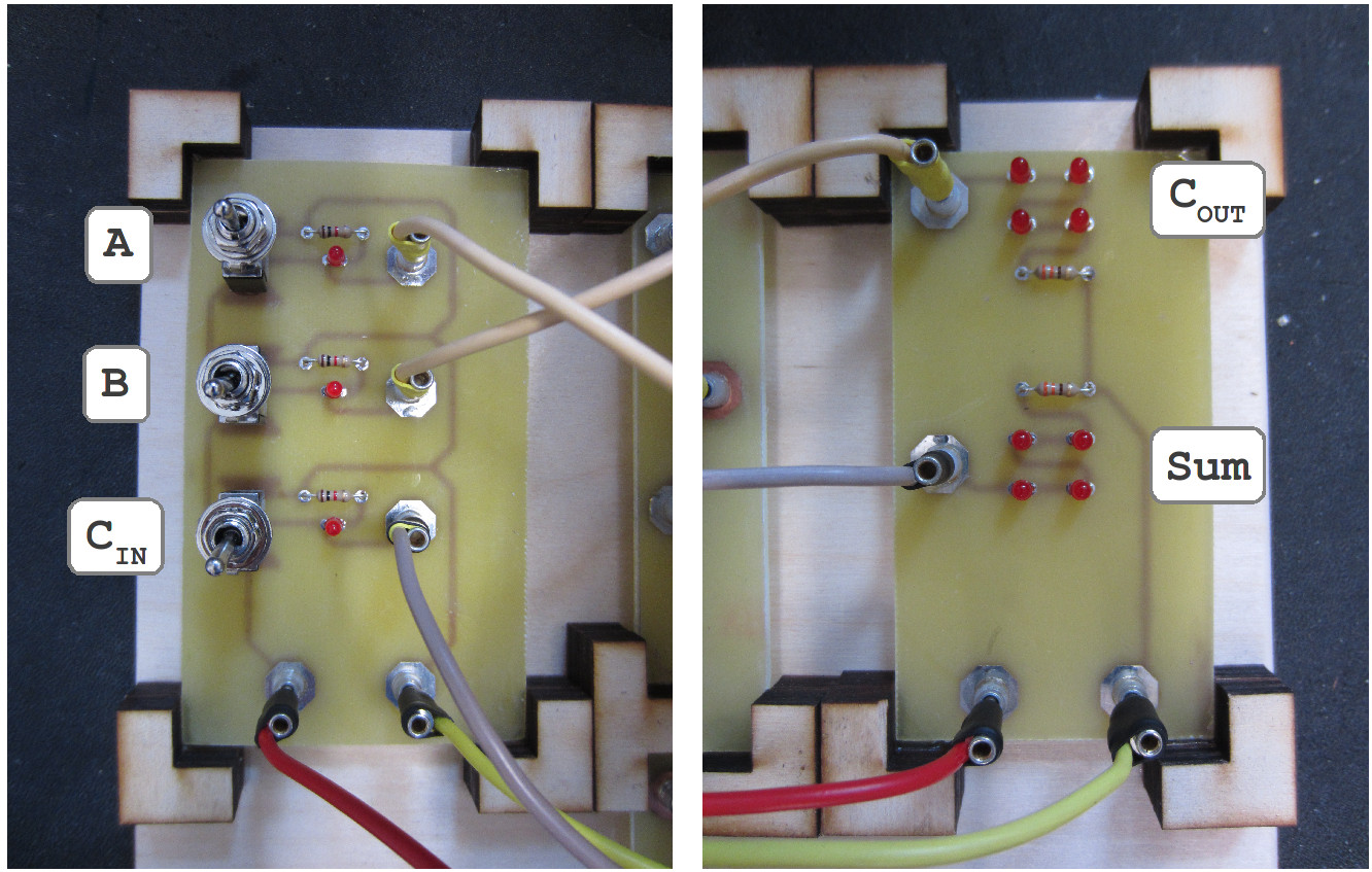
Figure 13 : Switch board (left), LED board (right)
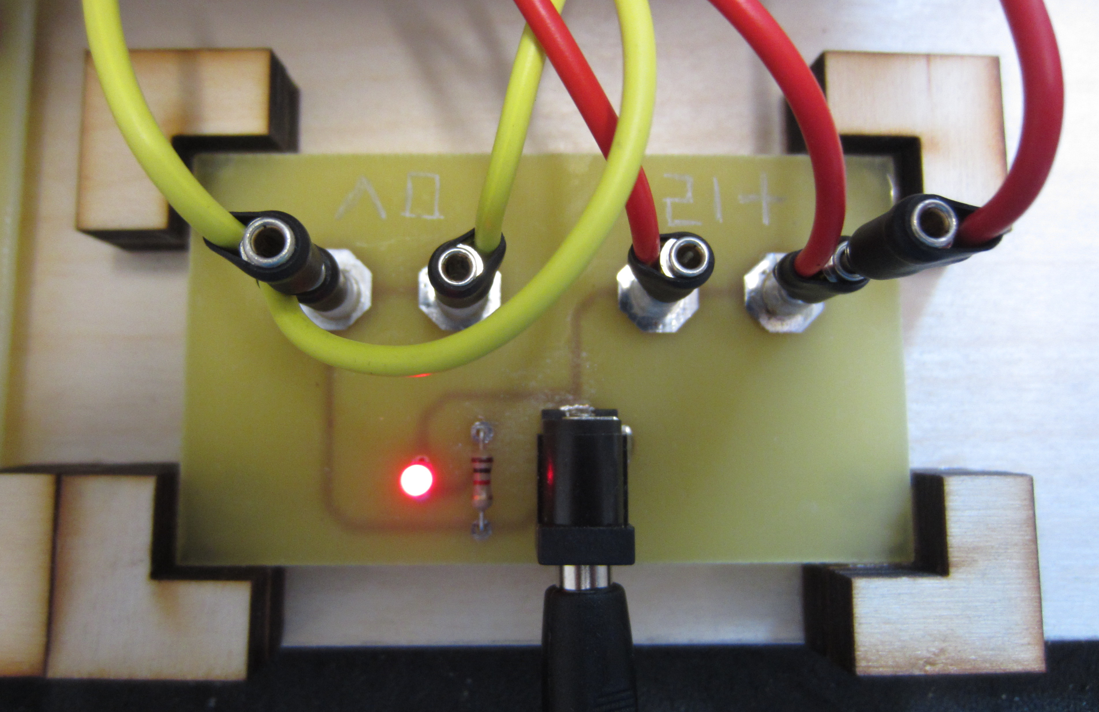
Figure 14 : DC power board
Now Flip-flops .....
WORK IN PROGRESS

This work is licensed under a Creative Commons Attribution-NonCommercial-NoDerivatives 4.0 International License.
Contact email: mike@simplecpudesign.com