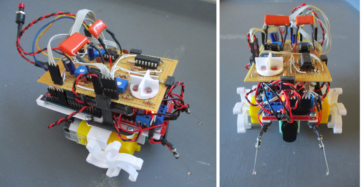
Figure 1 : robot cockroach
To support the computer architectures module i teach, i developed a series of weekly exercise sheets. These were divided into two parts, the first covered your typical bookwork type topics, a chance to practice the fundamental material taught in lectures e.g. converting between number bases, binary addition etc. The second part focused on showing how this knowledge could be applied / used in a real world context, the fun bit :). As always, following the bug theme, i felt it was appropriate to create a robot cockroach, to counter the previous bug trap. This project shows how you can use Boolean algebra and simple logic gates (INV, AND, OR, XOR) to implement a fully configurable controller based on a subsumption architecture (Link), with multiple distinct behaviours, all implemented in a Xilinx XC9572XL CPLD (Link)(Link). This web page talks through the design and development of this robot, a series of digital design tasks (answers are below tasks, so if you don't want to see the solutions, don't read to far) and some instructions on how you can create and build your own robot.
Actuators : H-bridge, motors.
Combinatorial logic circuits : control logic.
Encoders and decoders : LDR compound eye.
Sensors : bump switch.
Flip-Flops : explore behaviour.
State machine 1 : follow light behaviour.
State machine 2 : obstacle avoidance behaviour.
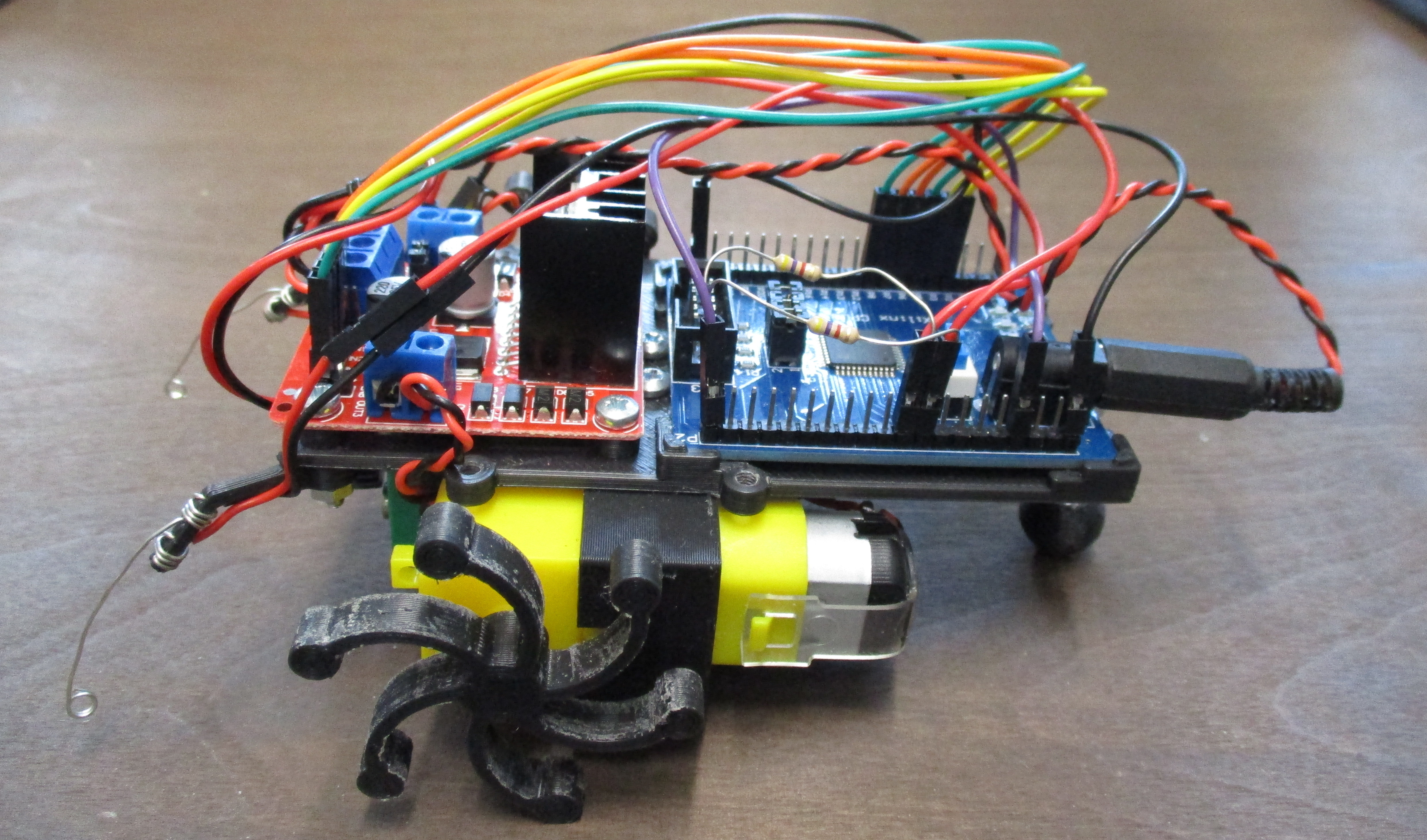
CPLD board: complex programmable logic device.
Motor control board : h-bridge and regulator.
Sensor interface board : 555 timer and voltage comparator.
Chassis : building the 3D printed chassis.
Testing : Xilinx ISE project files
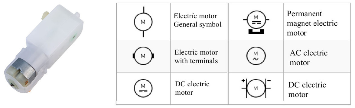
Figure 2 : DC motor (left), electrical symbols (right)
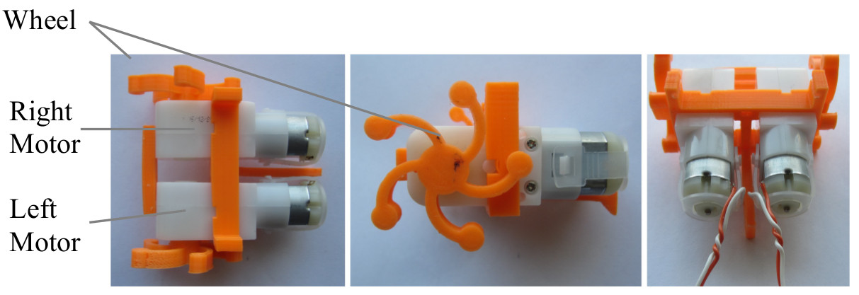
Figure 3 : DC motors mounted on chassis (top, side and back views)
IMPORTANT, any inductive load i.e. a coil of wire, is capable of storing large amounts of energy in its magnetic field. When the voltage producing this field is turned off the magnetic field will collapse, generating a very large voltage spike. Therefore, we need to add suppression circuits to prevent this transient from damaging the drive MOSFETs and other digital circuits. These are not shown in the H-bridge circuit, but will be included in the final design. Always ensure you are using the correct drive circuits if you are connecting relays, solenoids or motors to a CPLD, Raspberry Pi or Arduino etc.
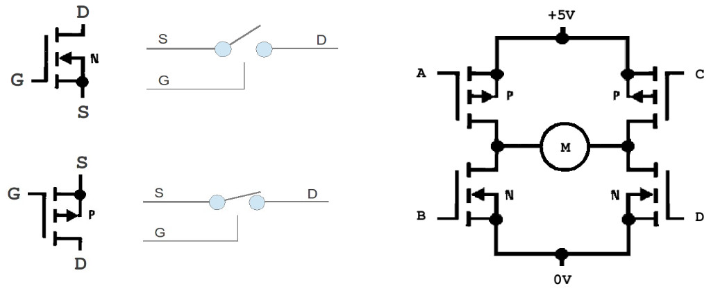
Figure 4 : MOSFETs (left), H-Bridge driver (right)
This drive circuit uses P-channel (normally closed) and N-channel (normally open) transistors. The four transistors are controlled using inputs: A, B, C and D. By turning on the correct transistor pairs we can control the direction of applied voltage across the motor i.e. the direction of rotation, as shown in figure 5. If all transistors are turned off i.e. open state, the motor is disconnected and will freewheel. If the bottom two N-channel transistors are turned on, both motor terminals are connected to 0V i.e. are connected together. If the motor is now manually rotated and no voltage is applied, it will behaviour as a generator, producing a voltage that will oppose the direction of rotation i.e. it will implement regenerative breaking.
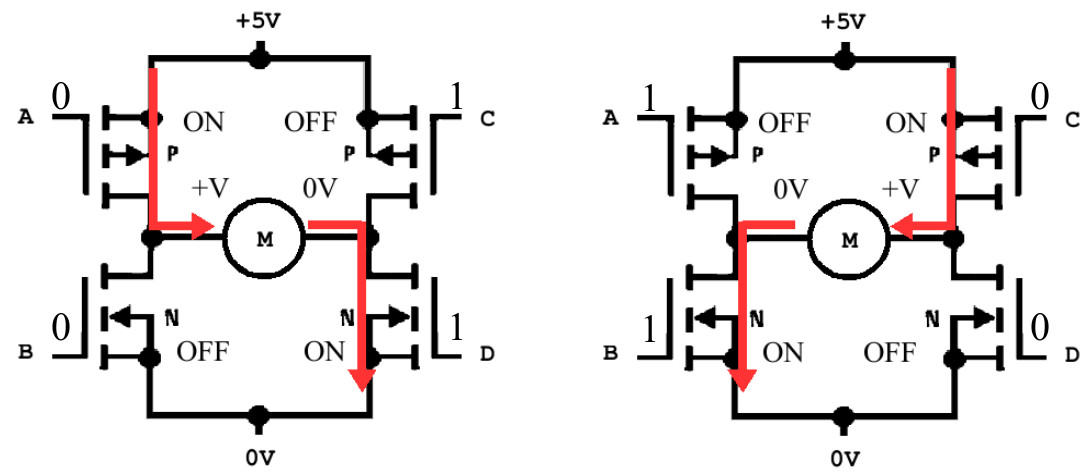
Figure 5 : H-Bridge operation, clockwise (left), anti-clockwise (right)

Figure 6 : H-Bridge truth table
Task : each motor state has been assigned a two bit control code (CTL1, CTL0), as shown in figure 6. Design a logic circuit to convert this two bit code into the four control signals: A,B,C and D, used to drive the MOSFETs. Hint, two of the control signals do not require any logic. The other two can each be produced using two two-input logic gates.
Note, when using a H-bridge you need to ensure that transistors in the same column i.e. transistors A and B, or C and D, are never turned on at the same time as this will cause a short circuit across the battery and will damage the transistors. The circuit designed in the previous task ensures that this can not occur. Alternatively we could implement this functionality in software using a processor, however, this may not be a good idea e.g. during the boot process your software is not controlling these signals, therefore, there is a possibility that bad things could happen. When designing hardware its always a good idea to play safe, if there is a possibility that things could go wrong they probably will. You can only blow-up hardware once :).
Answer: a simple process of visual inspection, we have two inputs (CTL1, CTL0) and four outputs (A,B,C,D). You need to work on one output at a time, asking the question how can i use the input values to generate the required outputs. The easy ones to spot are B and D, if you look at their outputs you can see that these are the same as CTL1 for B and CTL0 for D, therefore, no logic required. For A and C we can spot that there is only one input state that generates a logic 0, therefore, we can design a logic circuit accordingly, as shown below.
A =  CTL1 + !CTL0
B =  CTL1
C = !CTL1 + CTL0
D =  CTL0
Note being an electronics engineer at heart i use electric notation in my Boolean equations i.e NOT = !, OR = +, AND = & and just to confuse mathematicians XOR = ^. Always check your / my answers, i have been know to make the odd typo :). For each input state i.e. 00,01,10 and 11, check that each equation produces the output defined in its truth table.
To allow the robot to move in an arc we need to vary the speed of each motor e.g. if the left motor is running at 50% speed and the right motor 100% the robot will arc left. Speed control can be achieve using pulse width modulation (PWM), as shown in figure 7. This signal can be used to switch the motor's state between rotating and freewheel i.e. when PWM=1 then rotate, when PWM=0 then freewheel. The longer the PWM signal is in the logic 1 state the faster the motor will turn. We will be looking at circuits to generate this oscillating signal in a later practical.
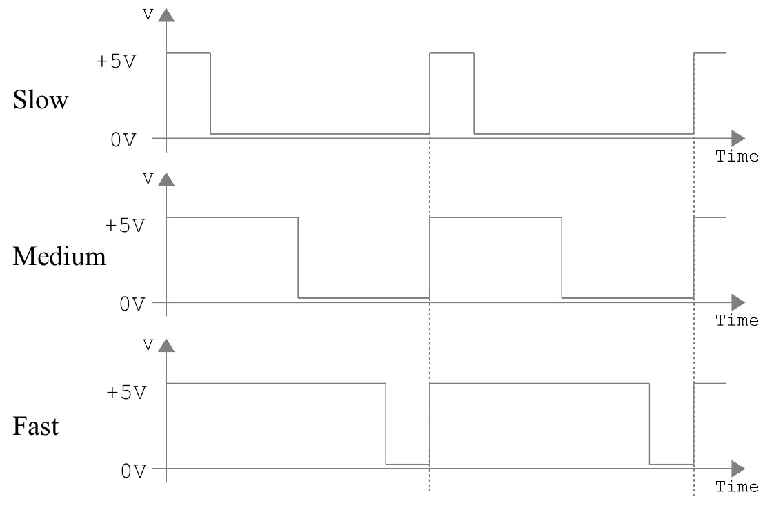
Figure 7 : Pulse width modulation (PWM)
Task : the previous H-bridge circuit has been modified to include four additional logic gates i.e. the “?” boxes, as shown in figure 8. What logic gates should be used in these boxes to implement the speed control functionality i.e. when PWM=1 control signals A,B,C and D are passed unaltered, when PWM=0 these control signals are masked and the transistors set to the freewheel state, as defined in figure 6.
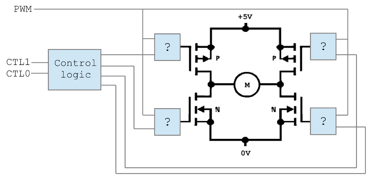
Figure 8 : modified H-bridge
Answer: the key point to note here is that the H-bridge uses two types of transistors: N-channel and P-channel (look for small N and P in circuit diagram, or circuit symbol). A N-channel transistor is turned on (switch closed) when a logic 1 is applied to its gate. A P-channel transistor is turned on when a logic 0 is applied to its gate. Therefore, to turn off these transistors, allowing the motor to free-wheel, we need to set the N-channel gates to logic 0 and the P-channel gates to a logic 1. Therefore the previous logic equations can be updated to:
A =  (CTL1 + !CTL0) + !PWM
B =  CTL1 & PWM
C = (!CTL1 + CTL0) + !PWM
D =  CTL0 & PWM
Note: anything ANDed with 0 is 0, anything ORed with 1 is 1.
The directions of each motor can now be controlled using the logic circuits developed in the previous section. However, the control blocks that will be developing later specify a 3 bit movement command code, as listed in figure 9.
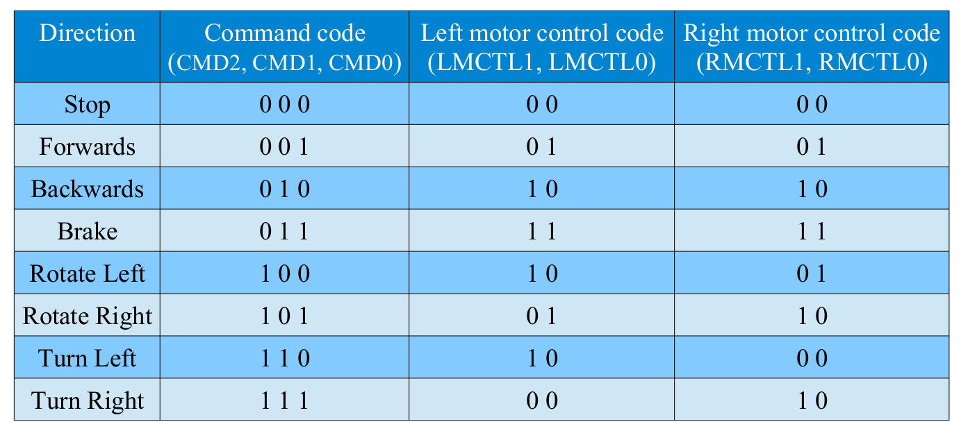
Figure 9 : Movement command codes
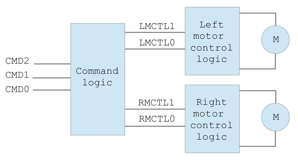
Figure 10 : movement logic block diagram
Task : each movement command has been assigned a three bit command code (CMD2, CMD1, CMD0), as shown in figures 9 and 10. Using only bit multiplexers design a logic circuit to convert this three bit code into the four H-bridge control signals: (LMCTL1, LMCTL0) and (RMCTL1, RMCTL0). The previously developed motor control logic truth table is shown in figure 11.
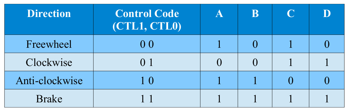
Figure 11 : H-bridge command codes
Hint, look at the mapping from input to output states, can you spot any similarities between(CMD1, CMD0) and (CTL1, CTL0)? The assigned command codes were not assigned randomly. If your not sure where to start a partially complete solution is shown below:
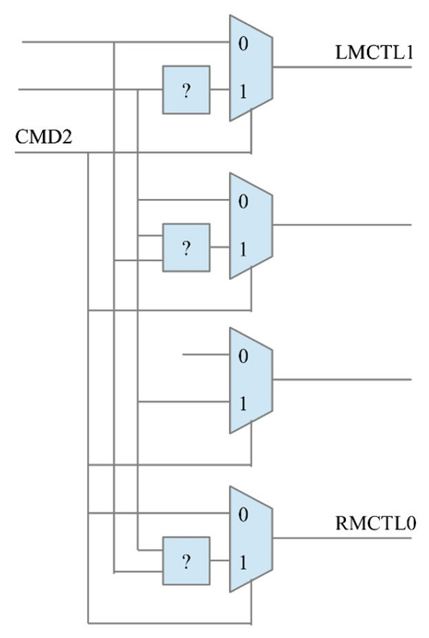
Figure 12 : movement logic - multiplexer implementation
Answer: again starting with visual inspection of the relationship between the three inputs (CMD2, CMD1, CMD0) and the four outputs(LMCTL1, LMCTL0) and (RMCTL1, RMCTL0). The trick here is to spot that when CMD2 is a logic 0, that both (LMCTL1, LMCTL0) and (RMCTL1, RMCTL0) are the same as (CMD1, CMD0). When CMD2 is a logic 1, LMCTL1 = !CMD0 and RMCTL1 = CMD0. Both LMCTL0 and RMCTL0 only have a single logic 1 when CMD2 is a logic 1 so we can design the logic to generate these states:
LMCTL1 =  (CMD1 & !CMD2) + (!CMD0 & CMD2)
LMCTL0 =  (CMD0 & !CMD2) + ((!CMD1 & CMD0) & !CMD2)
RMCTL1 =  (CMD1 & !CMD2) + (CMD0 & !CMD2)
RMCTL0 =  (CMD0 & !CMD2) + (!(CMD1 + CMD0) & !CMD2)
Using multiplexers to implement this command logic can simplify the design process, however, the resulting circuit will typically be less efficient i.e. will require more logic gates.
Note, as a general rule of thumb the more complex you make a circuit the higher the probability that the critical path delay will be increased i.e. the longest chain of logic gates from an input to an output. Increasing this delay slows down a circuits operation i.e. it will take longer for an output to reach a stable state. For a functional unit within a processor this increase can significantly reduce its processing performance. For the command logic developed here it will have little impact i.e. increasing the time to update the motor control signal by 100ns will not be noticeable, the motors can not respond that quickly, however, for a processor it would be devastating, significantly reducing its maximum clock speed.
To assess the efficiency of the multiplexer solution the same command logic can be implemented using the block diagram shown in figure 13.
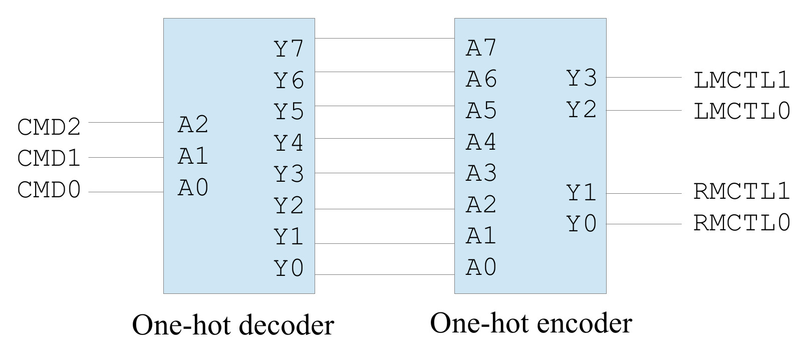
Figure 13 : movement logic - decoder block diagram
Task : design the logic circuits required to implement the one-hot encoder and decoder shown in figure 13. If your not sure where to start a partially complete solution is shown below:
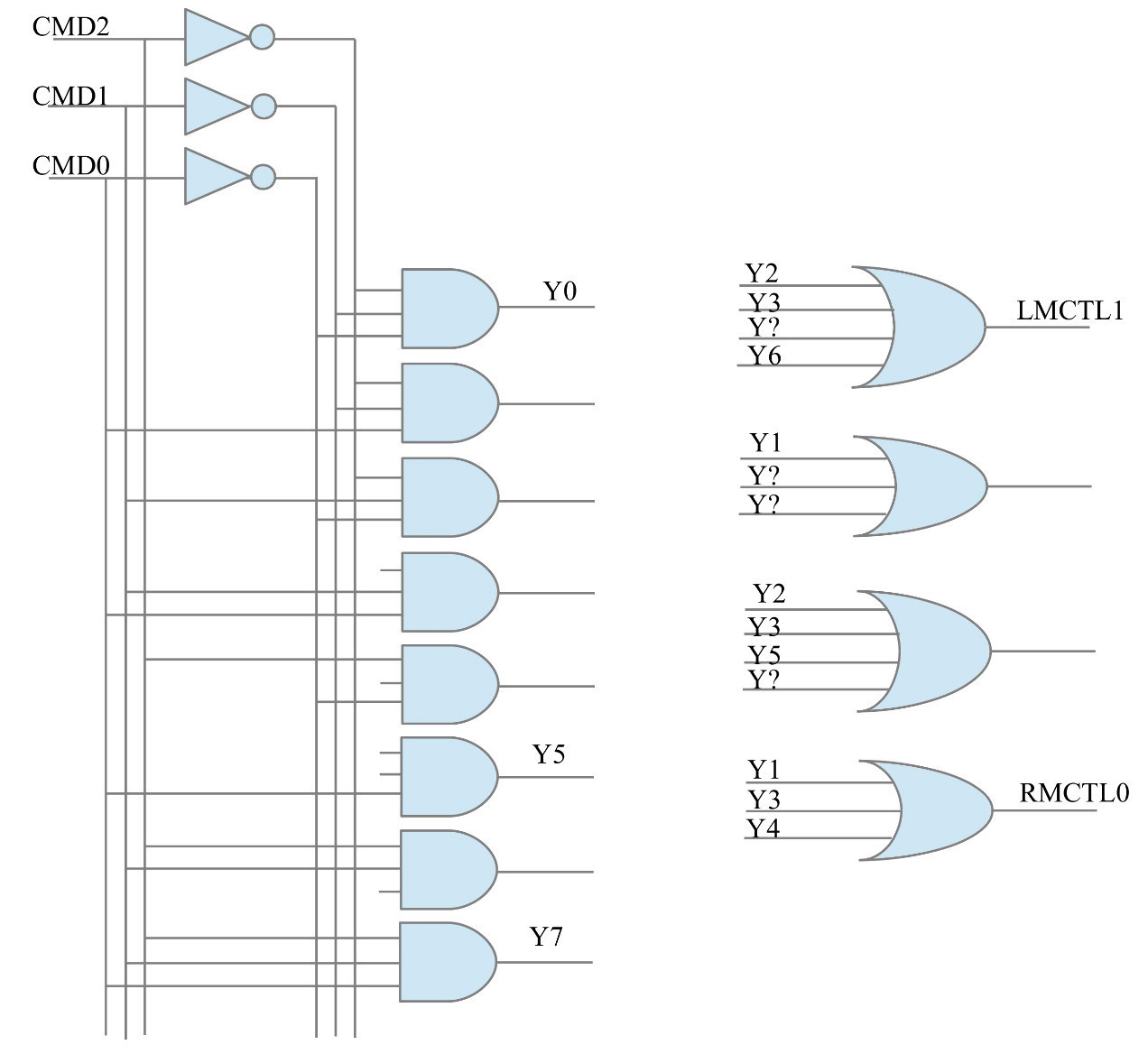
Figure 14 : movement logic - decoder implementation
Answer: this type of logic design can again be performed using visual inspection. The one-hot decoder has an output for each input state i.e. Y0 - Y7, therefore, all we need to do is for each output identify which states output a logic 1 and simply OR these together to produce the required output, as shown below:
Y0 = !CMD2 & !CMD1 & !CMD0
Y1 = !CMD2 & !CMD1 &  CMD0
Y2 = !CMD2 &  CMD1 & !CMD0
Y3 = !CMD2 &  CMD1 &  CMD0
Y4 =  CMD2 & !CMD1 & !CMD0
Y5 =  CMD2 & !CMD1 &  CMD0
Y6 =  CMD2 &  CMD1 & !CMD0
Y7 =  CMD2 &  CMD1 &  CMD0

LMCTL1 = Y2 + Y3 + Y4 + Y6
LMCTL0 = Y1 + Y3 + Y5
RMCTL1 = Y2 + Y3 + Y5 + Y7
RMCTL0 = Y1 + Y3 + Y4
Task : calculate the number of logic gates used to implement the block diagram shown in figure 13/14 and for the multiplexer based solution in figure 12. Which implementation uses the most logic gates? If each logic gate takes 20 ns to process a change on its inputs i.e. its propagation delay, calculate the critical path delay for each solution. Which implementation is the quickest?
Answer: simply count the number of logic gates a signal needs to pass through to get to an output e.g. for the RMCTL0 output, the CMD1 signal needs to pass through a OR, then a NOT, then a AND and a final OR to update its output. Therefore, we see that the MUX implementation has a critical path of 4 gates, so a delay of 80ns. The decoder implementation has a shorter critical path of 3 gates, therefore, a smaller delay of 60ns. Note, this does depend on how you implement each logic gate e.g. logic gates with more that two inputs, NOR / NAND gates etc.
RMCTL0 =  (CMD0 & !CMD2) + (!(CMD1 + CMD0) & !CMD2)
                         4  2      1       3
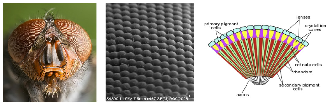
Figure 15 : compound eye
A robot is only as good as its sensors, it needs to be able to detect changes in its environment to take the appropriate actions. Sensors range from the complex: video camera, to the simple: bumper switches, with matching processing requirements i.e. a switch's state is typically represented by 1-bit, a camera with 640×480 RGB pixels will need to process 921600 bytes of data. The processing times associated with these sensors will affect the reaction time of the robot i.e. the time needed to capture, process and update the system's state. Therefore, to ensure that the system's real time processing requirements are meet either specialised hardware must be used or less data must be processed. A compound eye can be an alternative to a video camera, as shown in figure 15. These are based on an array of simple photoreceptors, giving the robot a low resolution, wide field of view image.
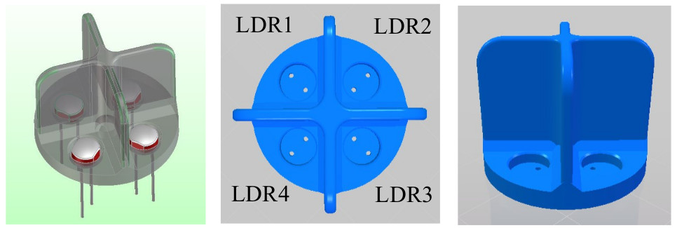
Figure 16 : LDR array (http://www.thingiverse.com/thing:859602)
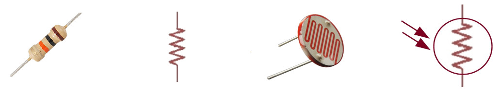
Figure 17 : Resistor (left) LDR (right), package and circuit symbol
To implement a very simple compound eye Light Dependent Resistors (LDR) could be used, as show in figure 16. This module contains four LDR sensors i.e. four pixels. An LDR is an electronic device who's resistance varies with light levels. When combined with a fixed resistor these will form a potential divider circuit, producing four continuous signals i.e. four analogue voltages, or greyscale values. The resistance of a component can be measured by observing the relationship between the voltage across the component and the current flowing through it i.e. Ohms Law:

Figure 18 : Ohms law
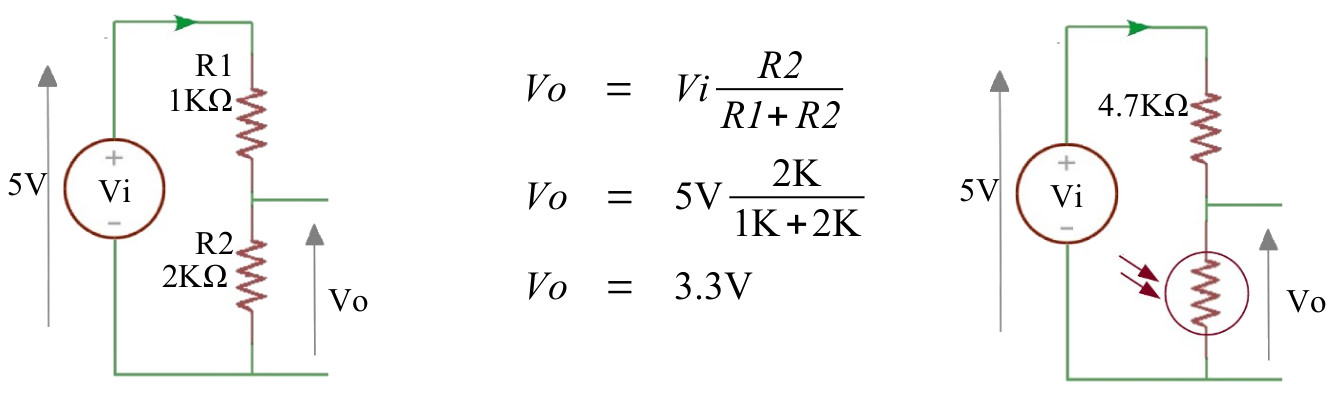
Figure 19 : Potential divider circuit
Resistors reduce the flow of current in a circuit. The amount of resistance a materiel has is measured in Ohms (Ω), conductors (metals) have a low resistance (0.1Ω), insulators a high resistance (10MΩ). This property is used in potential divider circuit to control a voltage source's output Vo, as shown in figure 19. The left hand circuit has two fixed resistors (1KΩ and 2KΩ) and is used to reduce a 5V source to 3.3V, using the middle formula i.e. the potential divider theorem. If we replace R2 with an LDR we now have a voltage output that is proportional to the light level. In normal lighting conditions the LDR's resistance is 4.7KΩ. In dark conditions this increases to 100KΩ and in bright conditions reduces to 100Ω. Therefore, using the above formula the output voltage of each sensor can be calculated. In normal light levels this will be 2.5V and will vary from 0.1V (bright) to 4.8V (dark). To convert these analogue signals into discrete digital values an analogue to digital converter (ADC) is normally used. However, to save space and money, a cheap and cheerful solution is used in this system :). The LDR signals could be connected directly to a NOT gate, as shown in figure 20.
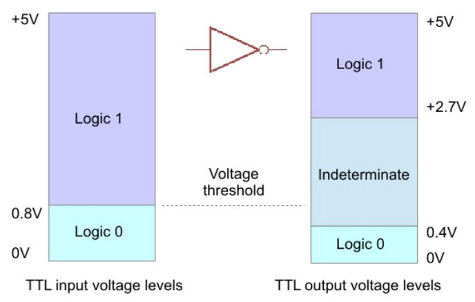
Figure 20 : NOT gate voltage threshold
The input voltage to the NOT gate will now no longer comply to the TTL logic standard i.e. it can be any value from 0V to +5V, rather than being in distinct voltage bands for a logic 1 or 0. The NOT gate only recognises that a signal is in a logic 0 state when its input voltage drops below 0.8V. Therefore, any voltage above this level is interpreted as a logic 1 i.e. the NOT gates behaviour is defined by a single voltage threshold. If the input is greater 0.8V output a logic 0, if the input is less than 0.8V output a logic 1 i.e. we have implemented a one bit ADC.
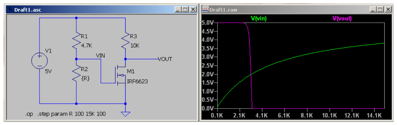
Figure 21 : simple threshold detector / inverter circuit
Note, the input voltage range from 0.8V to 2V for a TTL logic gate is defined as indeterminate. How a signal in this range is interpreted is dependent on the transistors used to constructed the logic gate. For the TTL logic gates used in this robot, this voltage range would typically be read as a logic 1.
Therefore, in normal lighting conditions the LDR signal (2.5V) will be interpreted as a logic 1, only entering the logic 0 state when a bright light is shone on the LDR (less than 0.8V). For the purposes of this robot thats not that useful. To adjust this voltage threshold the inverter circuit shown in figure 21 can be used. The MOSFET transistor is switched on when Vin (gate voltage) is greater than 2.0V. When the transistor is turned on, its resistance is approximately 1Ω (between drain and source), when off approximately 1MΩ. The SPICE simulation waveform shows the how the values of Vin and Vout change as R2 (LDR) is increased from 100Ω to 15KΩ. The voltage threshold of this circuit i.e. the sensitivity of these sensors, can be adjusted by changing the values of R1,R2 and R3.
Note, the fixed resistor R3 and the MOSFET transistor form a simple NOT gate. This circuit can again be considered as a potential divider, the output Vout can be calculated using the formula in figure 19. The equivalent circuits when the transistor is on and off are shown in figure 22. The triangle symbol, or GND is the same as 0V.
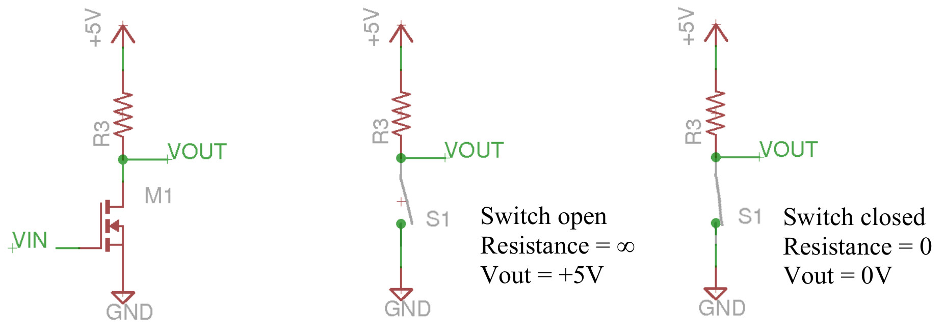
Figure 22 : inverter circuit (left), off (mid) on (right) equivalent circuits
Task : the four LDR signals: LDR1, LDR2, LDR3 and LDR4 are processed by a logic circuit, identifying the relative position of a bright object to the compound eye. Light positions will be classified using a 3bit binary code as shown in figure 23. Design a Boolean logic circuit to convert the LDR signals into this 3bit binary representation.
Note, the MOSFET inverter circuit shown in figure 21 is used to interface the LDR signals to the encoder i.e. this will output a logic 1 in light conditions and a logic 0 in dark conditions. Unused LDR states e.g. 1010 should map to code 000.
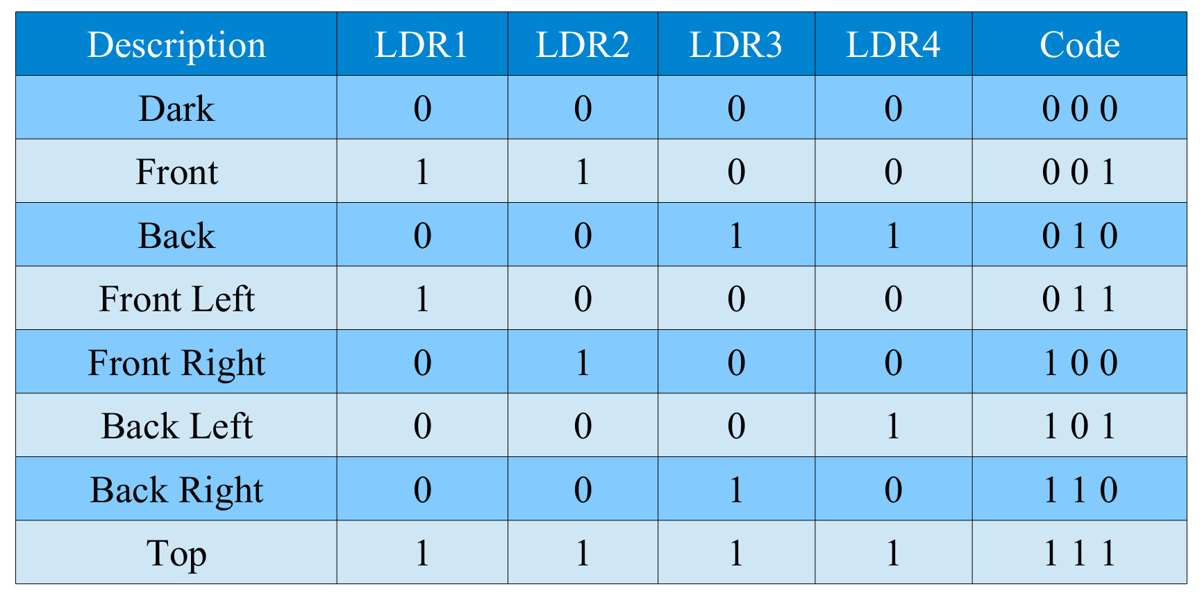
Figure 23 : LDR truth table
Answer: similar technique as the previous decoder, first generate a one-hot output for each valid state, then combine these states using OR gates to produce the required output code. Note, not all of the possible LDR input states are used. These inactive states will default to the 000 code i.e. will be interpreted to dark, this could be improved in future versions.
STATES
------
DK = !LDR1 & !LDR2 & !LDR3 & !LDR4
FT =  LDR1 &  LDR2 & !LDR3 & !LDR4
BK = !LDR1 & !LDR2 &  LDR3 &  LDR4
FL =  LDR1 & !LDR2 & !LDR3 & !LDR4
FR = !LDR1 &  LDR2 & !LDR3 & !LDR4
BL = !LDR1 & !LDR2 & !LDR3 &  LDR4
BR = !LDR1 & !LDR2 &  LDR3 & !LDR4
TP =  LDR1 &  LDR2 &  LDR3 &  LDR4

CODE
----
L3 = FR + BL + BR + TP
L2 = BK + FL + BR + TP
L1 = FT + FL + BL + TP
An early example of a bio-inspired robot is William Grey Walter's electro-mechanical tortoise, as shown in figure 24. Like the robot we are developing this robot had a photo-electric cell to detect light, but it also had a touch sensor i.e. a switch to detect if the robot had bumped into an obstacle during its travels. This central tilt switch was connected to the robots shell, such that if the robot's shell was to touch anything in its environment the robot would be able to detect this event and take avoiding actions.
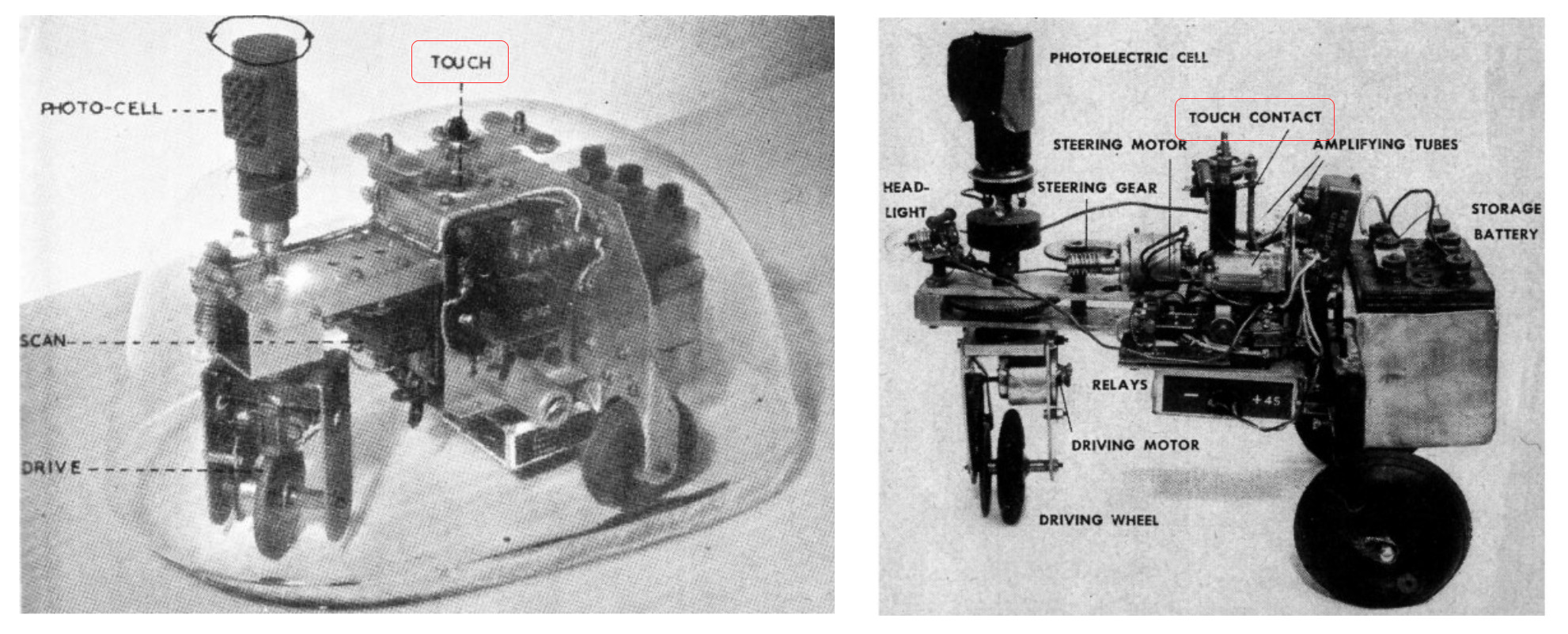
Figure 24 : electro-mechanical tortoise
This single bump switch helps reduce hardware requirements i.e. only need to process a single switch (signal). The disadvantage of this approach is that its difficult to localise the obstacle's position and take the appropriate actions. The robot can “guess” the probable obstacle location given its current state i.e. direction of movement, as shown in figure 25.
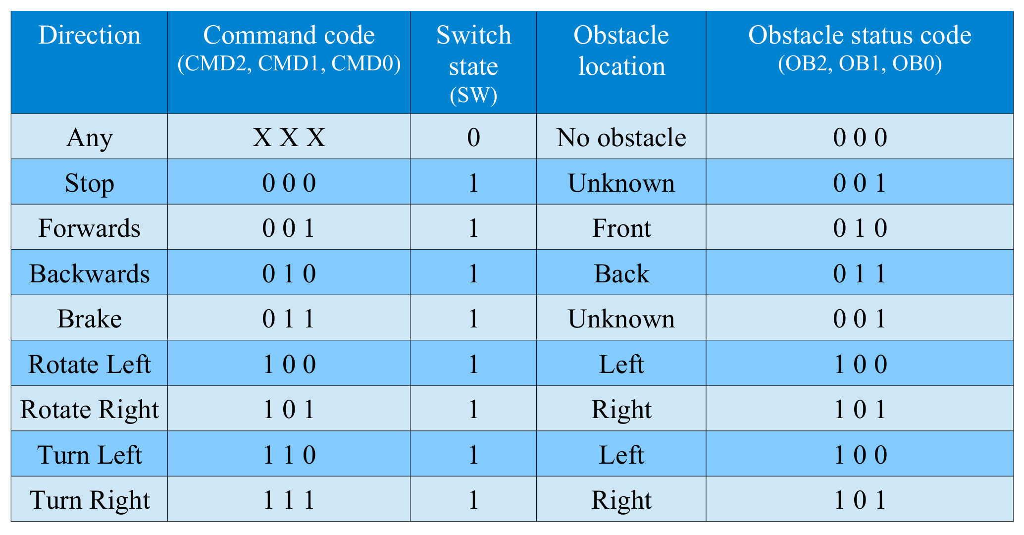
Figure 25 : Movement command codes
Task : design a Boolean logic circuit to convert the robot's state and switch signal into the three bit obstacle status code OB2, OB1 and OB0.
Hints : there are a number of different ways to go about designing this logic. As a first stab I would always start with visual inspection of the truth table, comparing the four bit input state (CMD2, CMD1, CMD0, SW) with the required output states (OB2, OB1, OB0). Below are descriptions of possible solutions, but can you spot which input signals are needed?
Answer: the required logic can be designed using visual inspection i.e. by examining the links between the four inputs (CMD2, CMD1, CMD0, SW) and the three outputs (OB2, OB1, OB0). Note, you can minimise these equation using more formal design techniques e.g. Boolean algebra (Link), or Karnaugh maps (kmaps) (Link), but visual inspection normally gets you most of the way for these simple circuits. Also, remember even if you don't quite get the smallest implementation the Xilinx tools will always automatically try to minimise this logic when it generates the configuration bit file.
OB2 = CMD2 & SW
OB1 = !CMD2 & (CMD1 ^ CMD0)
OB0 = (CMD2 & CMD0) + (!CMD2 & (CMD1 + !CMD0))
A behaviour control network will be used to implement the cockroach's brain. Sometimes called a Subsumption architecture, this approach was suggested by R. Brookes, as an alternative solution to the traditional world modelling / planning robot control paradigm. These controllers define a series of behaviours, each behaviour working in parallel, converting sensor inputs into actuator control signals. Behaviours are given a priorities, higher level behaviours can temporarily suppress lower level behaviours i.e. subsume their behaviour, as shown in figure 26.
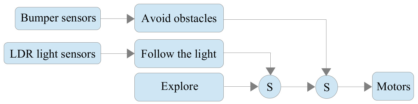
Figure 26 : subsumption architecture
Suppression points are indicated by circles, labelled with an 'S'. The important point to remember is that each behaviour is implemented as a state machine. All state machines are running in parallel. When a higher level behaviour becomes active it does not stop lower level behaviours, it only suppresses their outputs, replacing it with its own. Notes, the cockroaches behaviour could of been defined in a number of different ways, i went for this implementation to simplify construction and testing (i.e. just in case i needed to split the hardware over multiple devices).
Task : the robot's motors are controlled using a three bit code (CMD2, CMD1, CMD0). What hardware component could be used to implement each suppression point?
Answer: a 3-bit multiplexer.
This type of behaviour based control tightly couples sensor data to actuator actions i.e. a behaviour can be thought of as a simple reflex. This minimises processing, allowing the robot to respond very quickly to changes in its environment. Complex behaviours are created through the interaction of these simple behaviours i.e. suppression points. This method of defining a robot's behaviour allows an incremental development, new layers of behaviours can be added to the system without having to modify lower levels. Therefore, a key requirement to implement these types of controllers are sensors, as these systems do not have a world view (a map, knowledge of its environment it is moving through), all actions must be based on input sensor data. For this robot these will be:
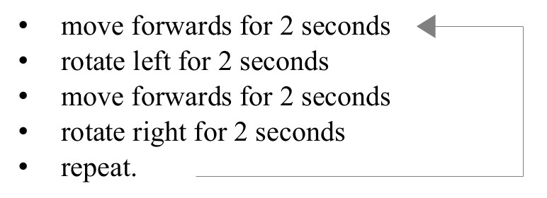
The base behaviour of the robot is explore. This can simply be a constant move forwards command, or it can be a series of movement commands implementing a defined search pattern, as shown in figure 27.
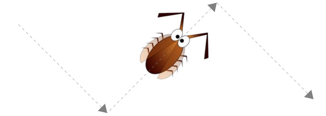
Figure 27 : search / movement pattern.
To control the robot's movements i.e. distance moved / angle turned, we could attach wheel encoders to each motor's drive shaft and measure their rotation i.e. knowing the drive wheel's circumference and the number of rotations performed we can calculate the distance moved or turned (inverse kinematics). For this robot the cost of these sensors would take the robot over budget :(, so a simpler approach will be taken: open-loop control. Assuming that the voltage applied to each motor is constant (a fully charged battery) and that the surface the robot is travelling across is level and flat, the distance travelled / angle turn will be proportional to time. From empirical observation it was found that performing a rotation command for 2 seconds causes the robot to turn approximately 90º, and that performing a move forwards command for 2 seconds will cause the robot to travel approximately 5cm. Therefore, implementing a 2 seconds delay in hardware will allow the robot to perform the type of search pattern previously shown.
The required 2 second delay will be implemented using a 555 timer, as shown in figure 28, producing a repeating square wave i.e. high for 1 seconds, low for 1 seconds, with an output frequency of 0.5Hz. For more information on how this circuit works refer to: (Link). Note, given the component values i had to hand the circuit shown will generate a 2Hz clock, this was divided down within the CPLD.
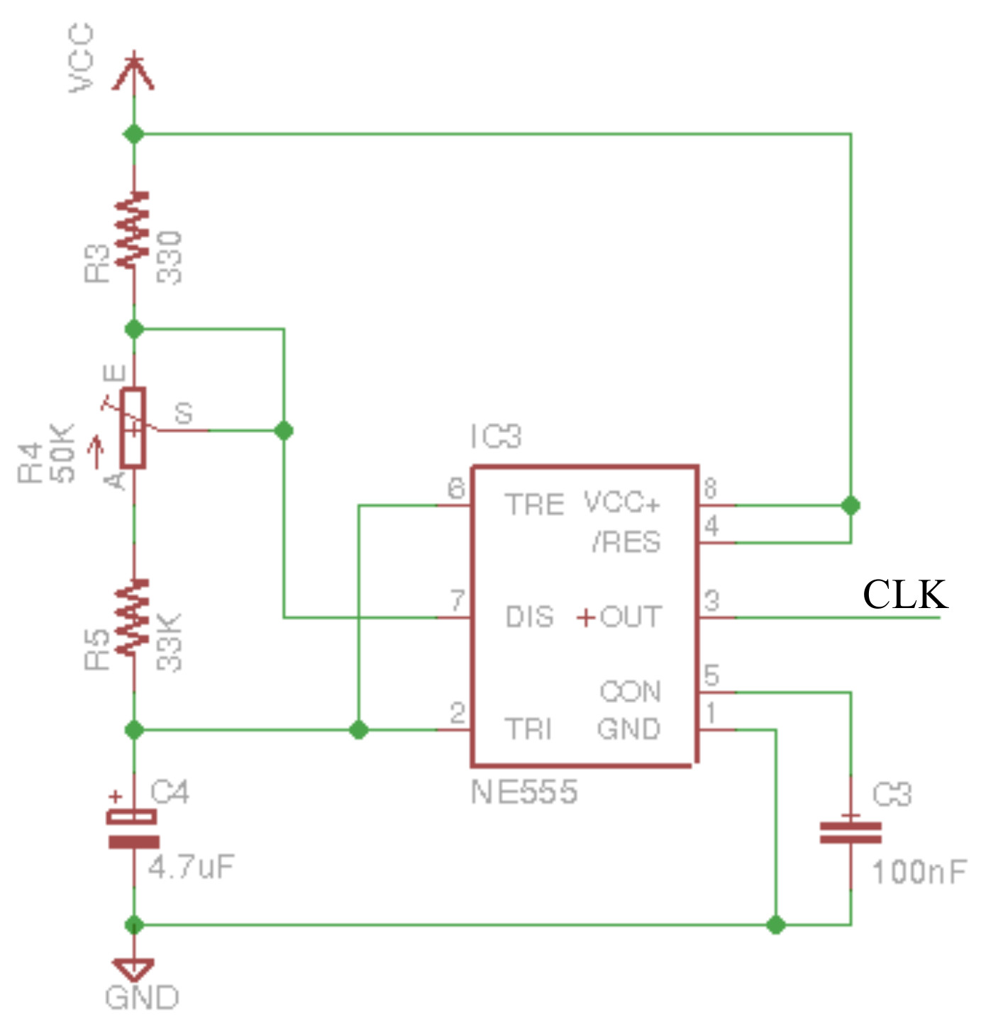
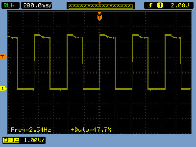
Figure 28 : 55 timer, astable multivibrator, circuit (top), scope trace (bottom)
The required sequence of movement command codes are shown in figure 29.
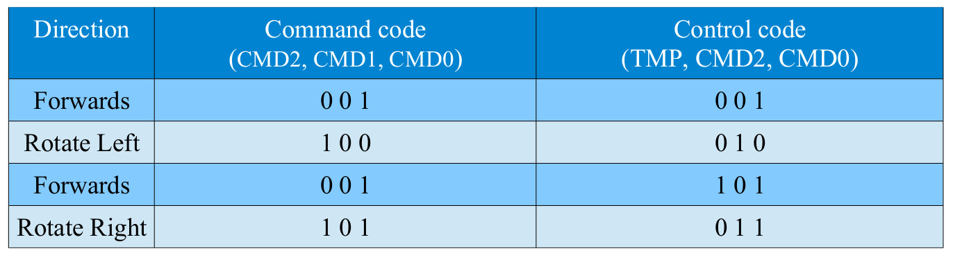
Figure 29 : control code sequence
From observation of these command codes it can be seen that CMD1 is constant, therefore, this signal does not need to be considered when designing this hardware i.e. it can be tied to a logic 0. To produce the required sequence generator each state within the explore behaviour has to have an unique encoding, which is a problem i.e. the two forwards commands have the same pattern. Therefore, after removing CMD1 an extra signal TMP will be added (not used to drive the motor controller) so that the control logic can differentiate between these two move forwards states.
Task : using the 555 timer to generate a 0.5Hz clock, can you see how the circuit shown in figure 30, can be used to generate the required sequence generator i.e. output patterns. Hint, output A=CMD0 and B=CMD2.
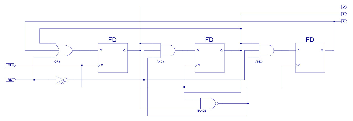
Figure 30 : sequence generator
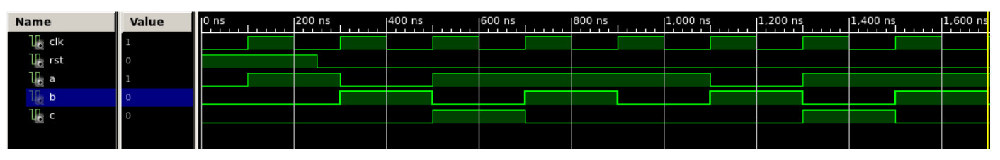
Figure 31 : sequence generator simulation
Answer : the first thing to note is that this circuit uses a synchronous clear. If the reset line (RST) is set to a logic 1 and the clock (CLK) pulsed, the output will be reset to A=1, B=0, C=0. Without this the required initial conditions will not be loaded into the flip-flops, so the circuit will not work. The next flip-flop states are determined by the three-input OR and AND gates:
Continuing the development of the subsumption architecture we will now implement the follow light behaviour. We have already developed the logic required to encode the LDR sensors, as shown in figure 23. Using this representation we will design and implement a state-machine to allow the robot to follow a beam of light e.g. in a dark room the cockroach will move towards bright objects, such as a window etc. The robots behaviour can be first described using the pseudo code below, each movement is defined using a 3bit movement command code shown in figure 9.
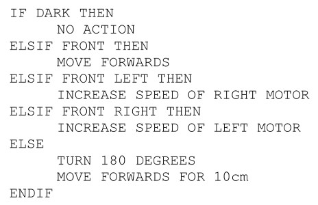
One possible implementation of these control rules is shown in figure 32. The state machine has six states: S0-S5, processing three inputs (L2, L1, L0) and controlling four outputs (MC(2:0), SPL, SPR, SEL).
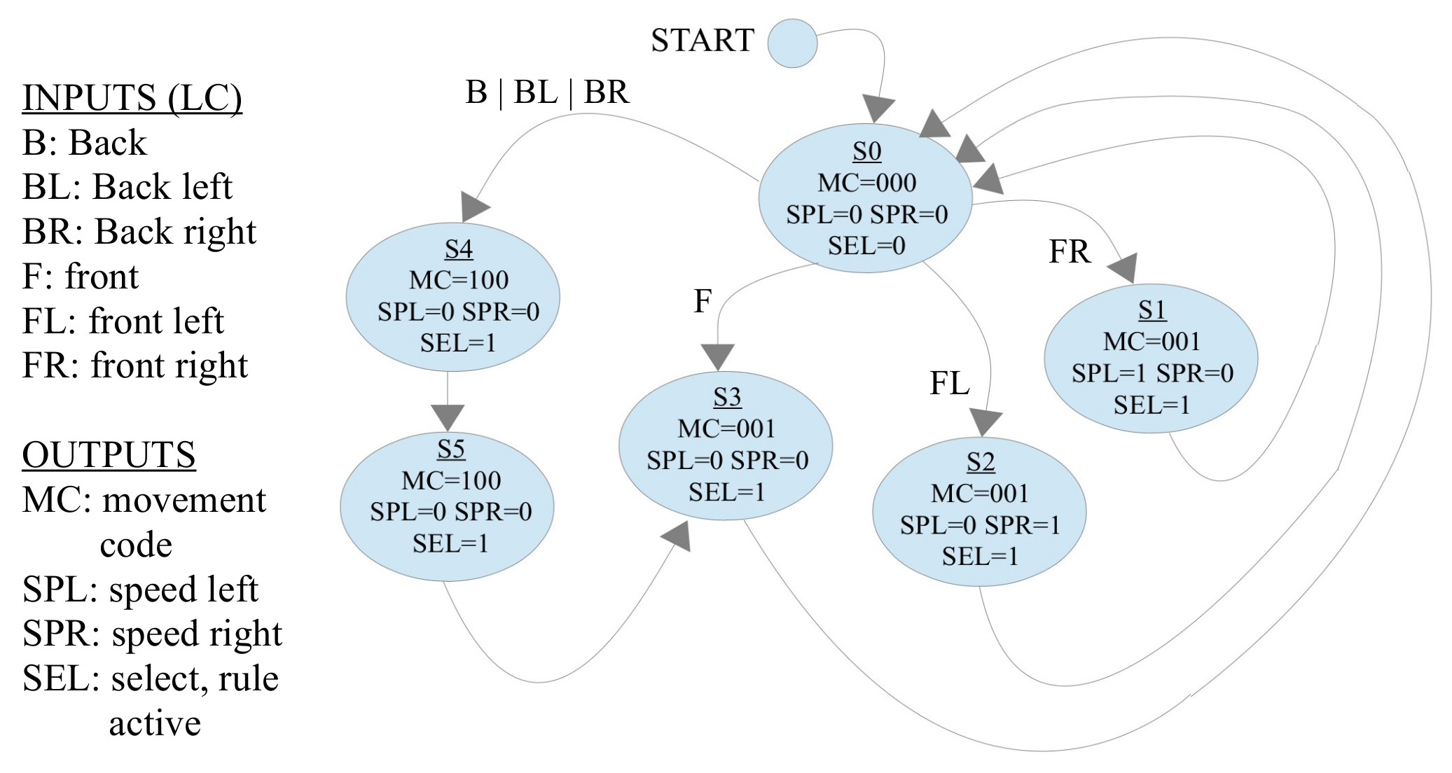
Figure 32 : follow light state diagram
As discussed in the Actuator section, the speed of a motor can be controlled using pulse width modulation (PWM). This signal could be generated using a ring counter, however, to save space in the programmable logic device (PLD) used to implement this robot ive moved this functionality into another 555 timer, as shown in figure 33.
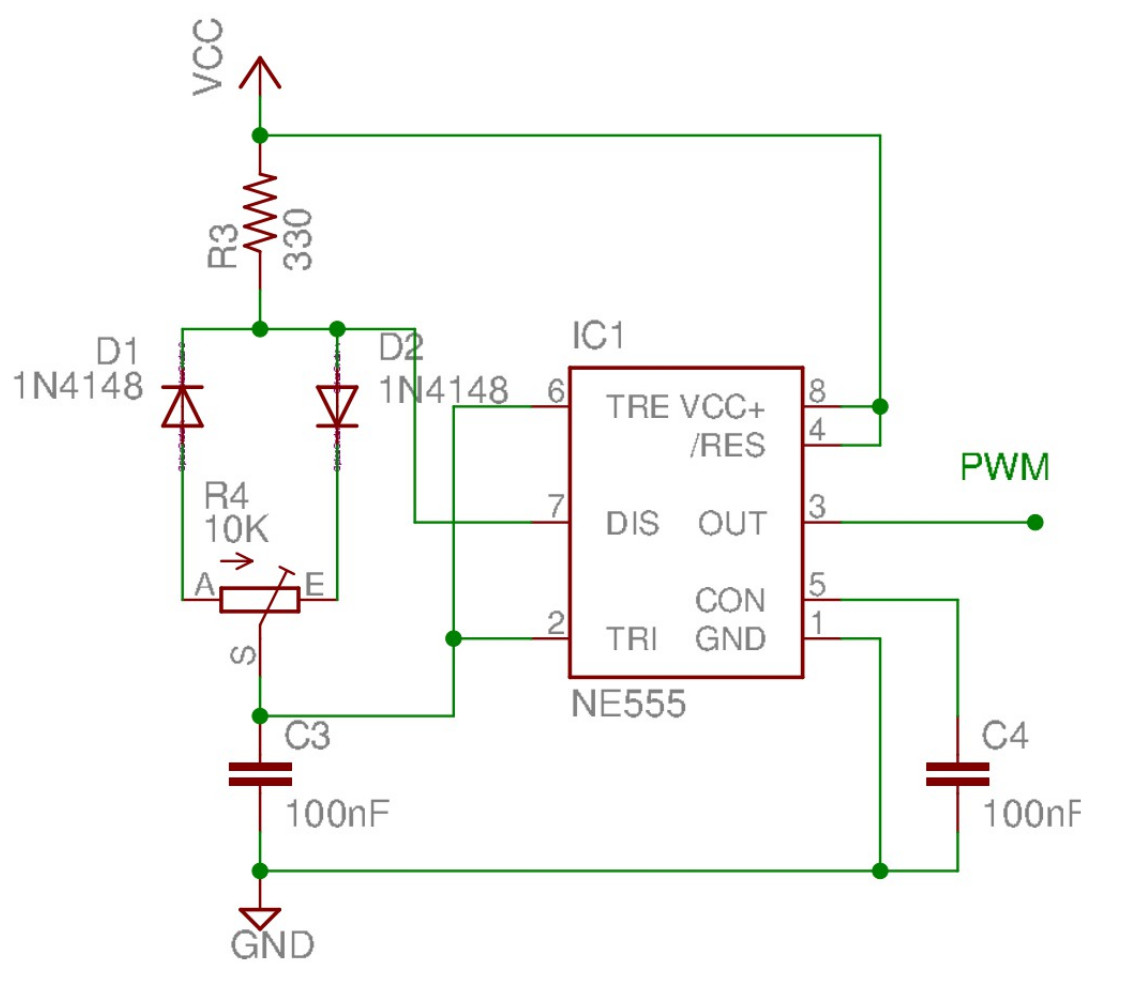
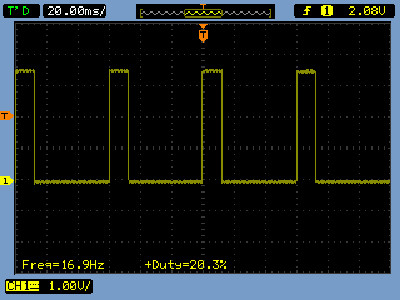
Figure 33 : 555 timer PWM, circuit (top), scope trace (bottom)
Note, in the final version the value of C3 was increased to 1uF to reduce the output frequency, this was done to improve low speed performance. This is because, if the output frequency is too high compared to current rise time, which is determined by the winding inductance i.e. LR, the output pulse from the PWM generator does not have enough time to produce a large enough magnetic field to cause rotation. You can identify this problem if the motor just makes a buzzzing sound.
This 555 timer generates a PWM signal i.e. by varying the variable resistor R4 we can control the mark-space ratio of the output PWM i.e. ratio of ON to OFF time. This signal can then be used within the PLD to switch the left or right motor to a lower speed i.e. outputs SPL and SPR. We will implement the state diagram in figure 32 as a Moore state-machine, using the block diagram shown in figure 34.
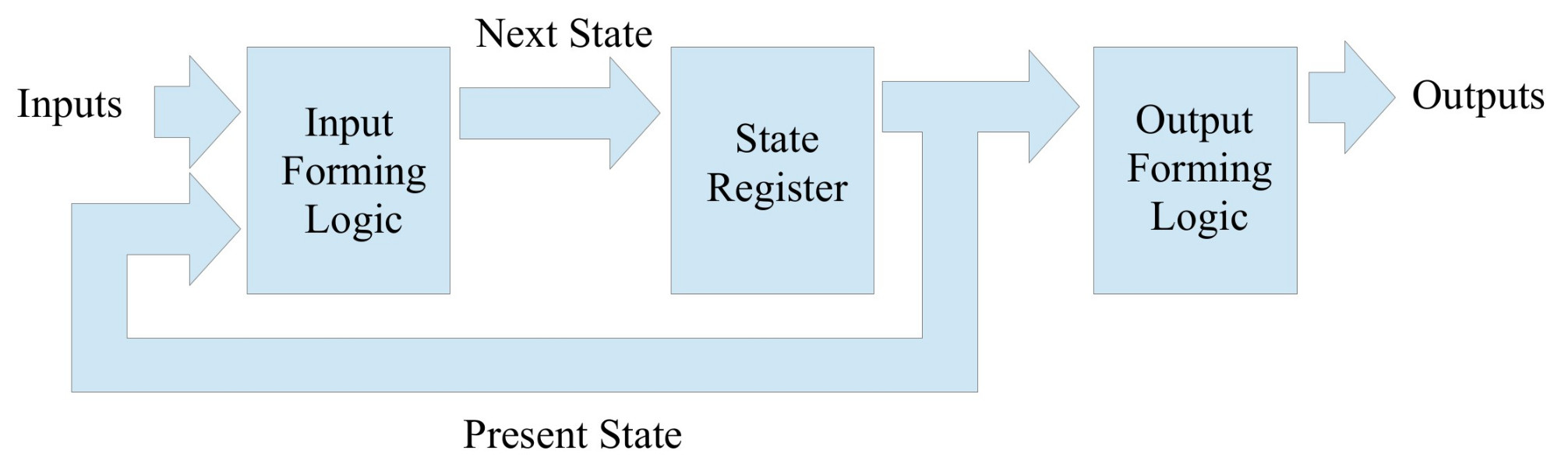
Figure 34 : Moore state-machine
Each state (S0-S5) is encoded using the following 3bit binary values:
This state value is stored in the state register i.e. three D-type flip-flops. The input forming logic controls the transition from one state to the next, based on the current state and input values. This can be represented by the truth table shown in figure 35.
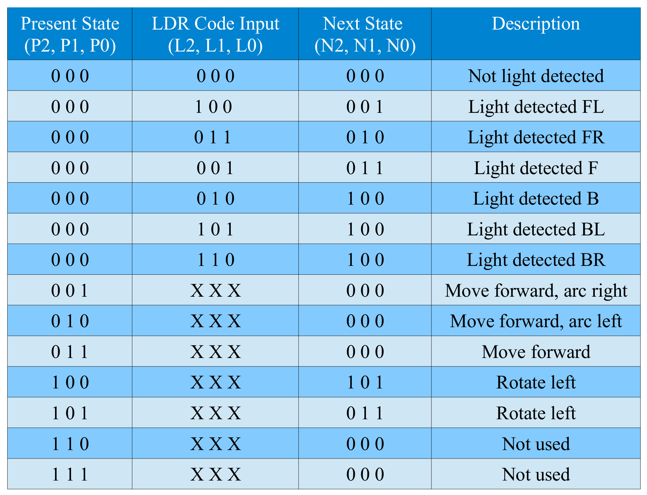
Figure 35 :Input forming logic truth table
From this we can derive the input forming logic, that generates the next state based upon the present state and the current input value e.g. if the state-machine is in state S0 (000) and the LDR inputs (L) detect a light source is front left (FL) (100), the input forming logic should output the next state value of S1 (001). Note, “XXX” mean don't care.
Task : the Boolean logic equations for the next state bits N2 and N1 are given below. Calculate the Boolean logic equation for N0.
N2 = !P2&!P1&!P0&!L2&L1&!L0 + !P2&!P1&!P0&L2&!L1&L0 +
     !P2&!P1&!P0&L2&L1&!L0  + P2&!P1&!P0

N1 = !P2&!P1&!P0&!L2&L1&L0  + !P2&!P1&!P0&!L2&!L1&L0 +
     P2&!P1&P0
Answer: N0 = !P2&!P1&!P0&(L2&!L1&!L0 + !L2&!L1&L0) + P2&!P1&!P0 + P2&!P1&P0
In a Moore state-machine outputs are determined by the current state not the inputs, this greatly simplifies the output forming logic truth table, as shown in figure 36.
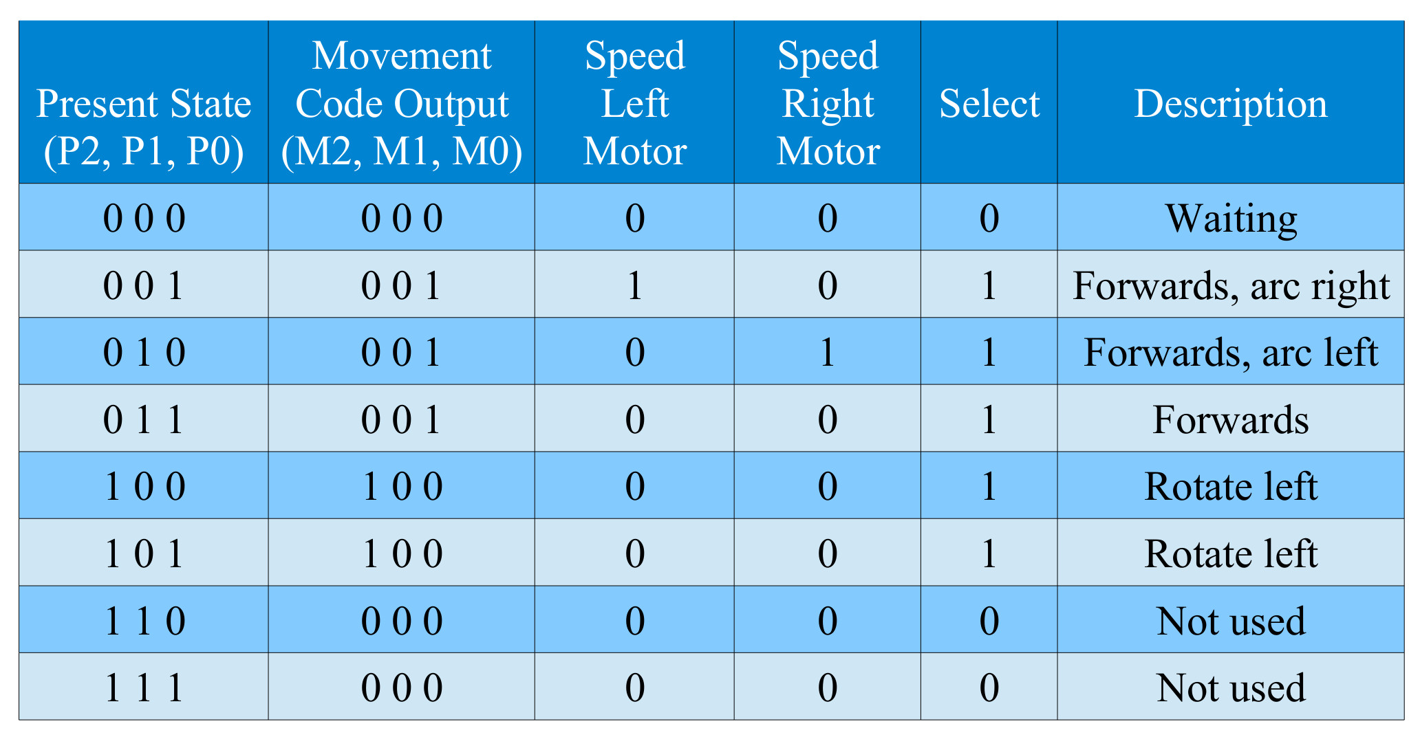
Figure 36 :Output forming logic truth table
By default each motor is operated at half speed. If the left or right motor speed signal (SPL and SPR) is set to a logic 1 that motor is switched to full speed.
Task : the movement command code (M), motor speed (SPL, SPR) and select (SEL) outputs are derived from the present state. The Boolean logic equations for Select, SPR, movement command code M0 are given below. Calculate the Boolean logic equation for : M1, M2 and SPL.
SPR = /P2.P1./P0
M0 = /P2./P1.P0 + /P2.P1./P0 + /P2.P1.P0
SEL = (P2+P1+P0).(/P2+/P1+P0).(/P2+/P1+/P0)
Hint, do you need any logic gates to generate output M1?
Answer: M2 = P2&!P1&!P0 + P2&!P1&P0, M1 = 0, SPL = !P2&!P1&P0
Note, the Boolean equations used to generate a truth table can be represented in a number of different ways. Consider the above SEL term, rather than using AND gates to generate the logic 1s, we have used OR gates to generate the logic 0s. These are called sum of products (SOP) and products of sums (POS) receptively. We now have all the required elements to implement this state-machine. The final circuit diagram is shown in figure 37. A simulation of this circuit is shown in figure 38.
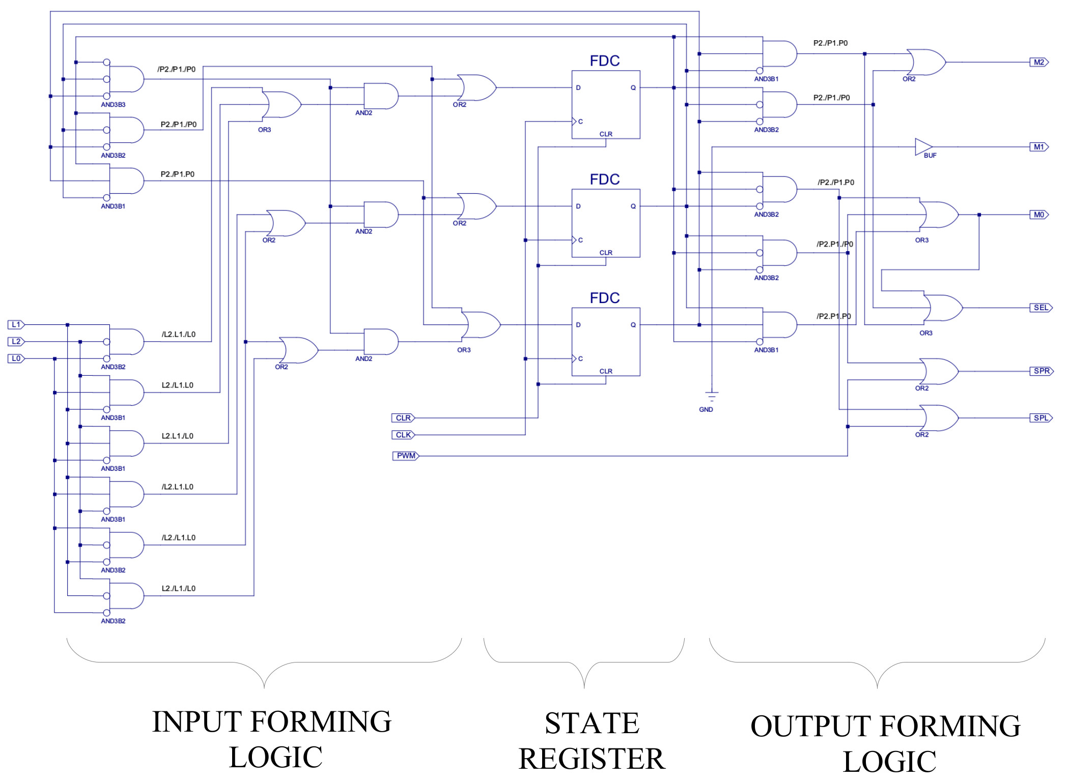
Figure 37 : follow light schematic
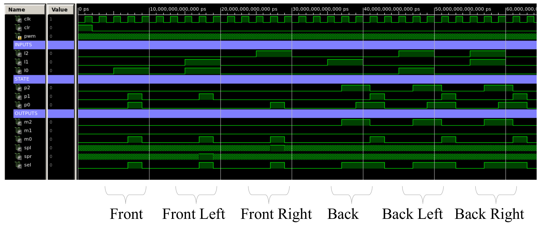
Figure 38 : follow light simulation
Task : examine the above circuit diagram and simulation, can you see how this circuit works?
Answer, the three D-type flip-flops (FDC) implement the state-machine's state register, the top flip-flop storing the present state P2, the next P1 and the bottom flip-flop P0. Apply the assigned state values to the Q outputs and confirm the correct outputs and next state values are generated to implement the state diagram shown in figure 32.
Continuing the development of the subsumption architecture we will now implement the avoid obstacles behaviour. To simplify the design, the number of bumper switches will be increased to two: Front Left (FL) and Front Right (FR). To reduce costs these will be implemented as basic wire contacts, interfaced using the simple potential divider circuit previously discussed, as shown in figure 39.
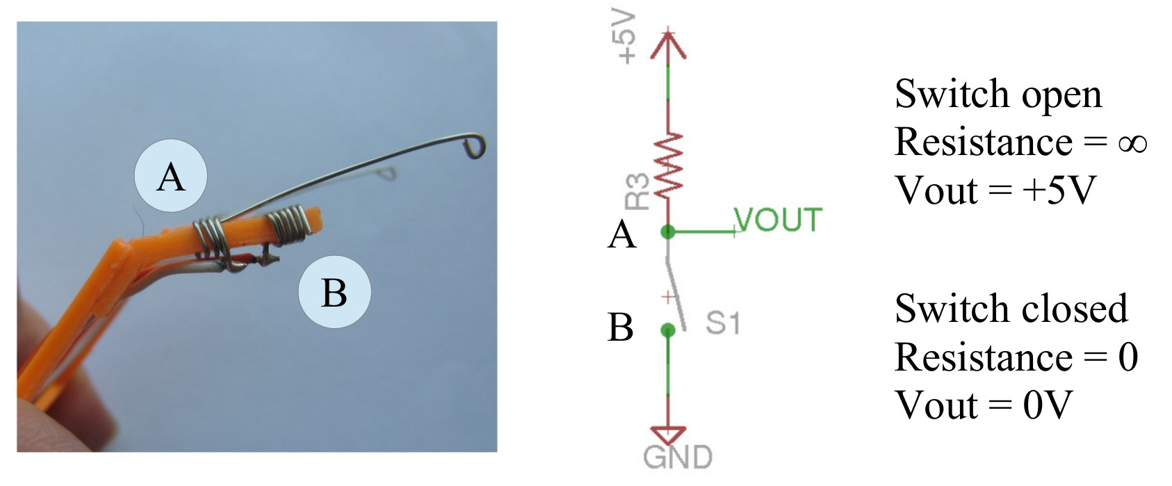
Figure 39 : bumper switch
Note, these are cheap and cheerful switches, not quite up to the job, but they do work. Long term probably best to replace these with micro-switches. Also, could add back bumper switches, these could then be used to update and improve these control rules.
Using these switches the robot can detect if the obstacle is on its left or its right and take the appropriate action. The behaviour of this state machine is defined by the pseudo code and state diagram shown in figure 40. The input forming logic truth table is shown in figure 41.
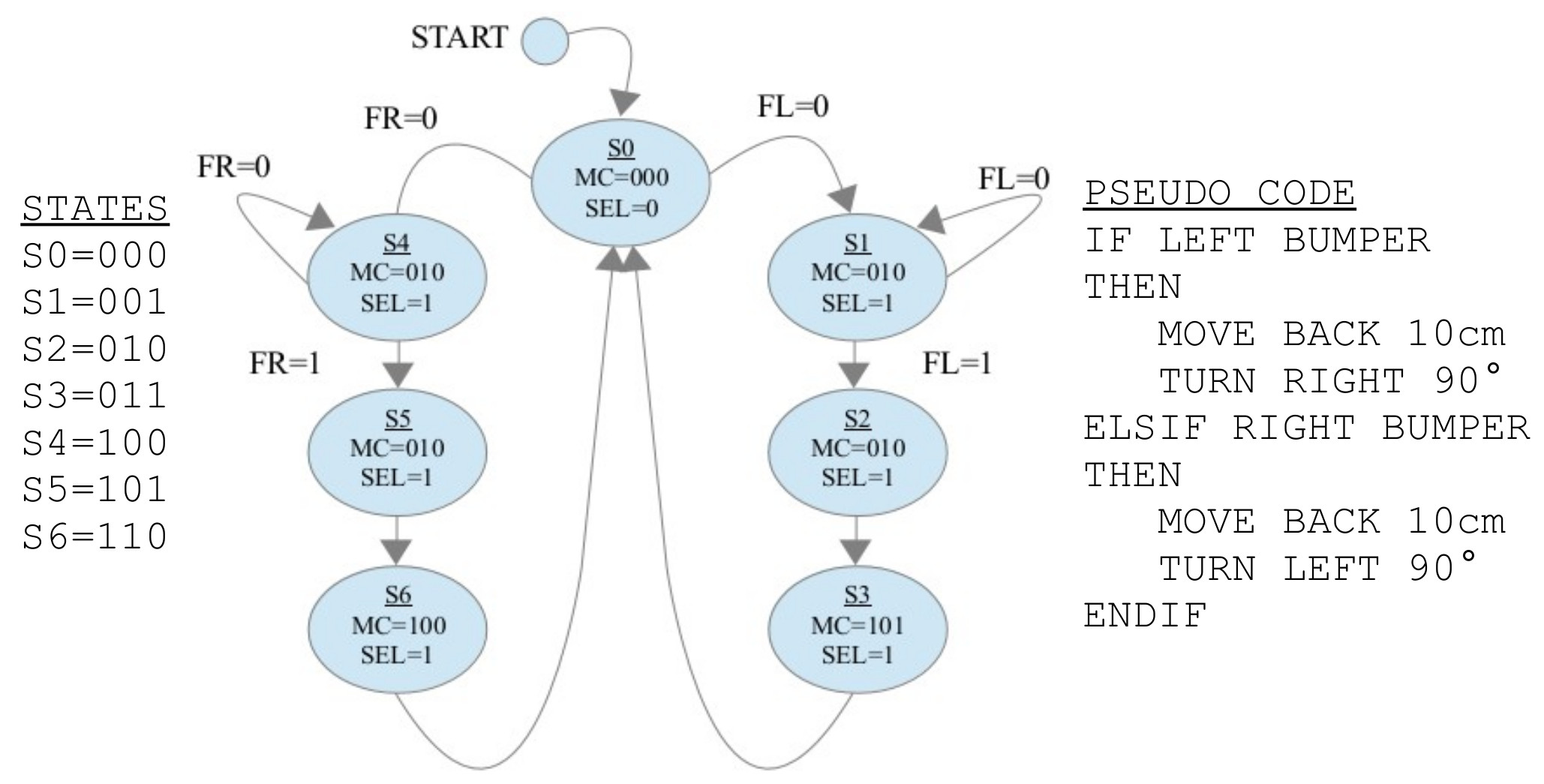
Figure 40 : avoid obstacles state diagram
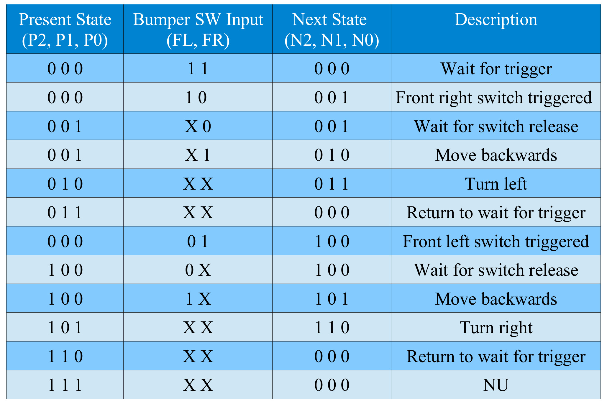
Figure 41 : Input forming logic truth table
The clock is again the 0.5Hz 555 timer discussed previously. Therefore, movements are again performed using open loop control i.e. the robot will turn 90° or move "5cm" during one clock cycle.
Task : implement the input forming logic described in figure 41. Then design the output forming logic and state register to complete the state diagram shown in figure 40.
Answer: same process as before, the final circuit diagram is shown in figure 42, input forming logic on the left, state register in the middle and output forming logic on the right.
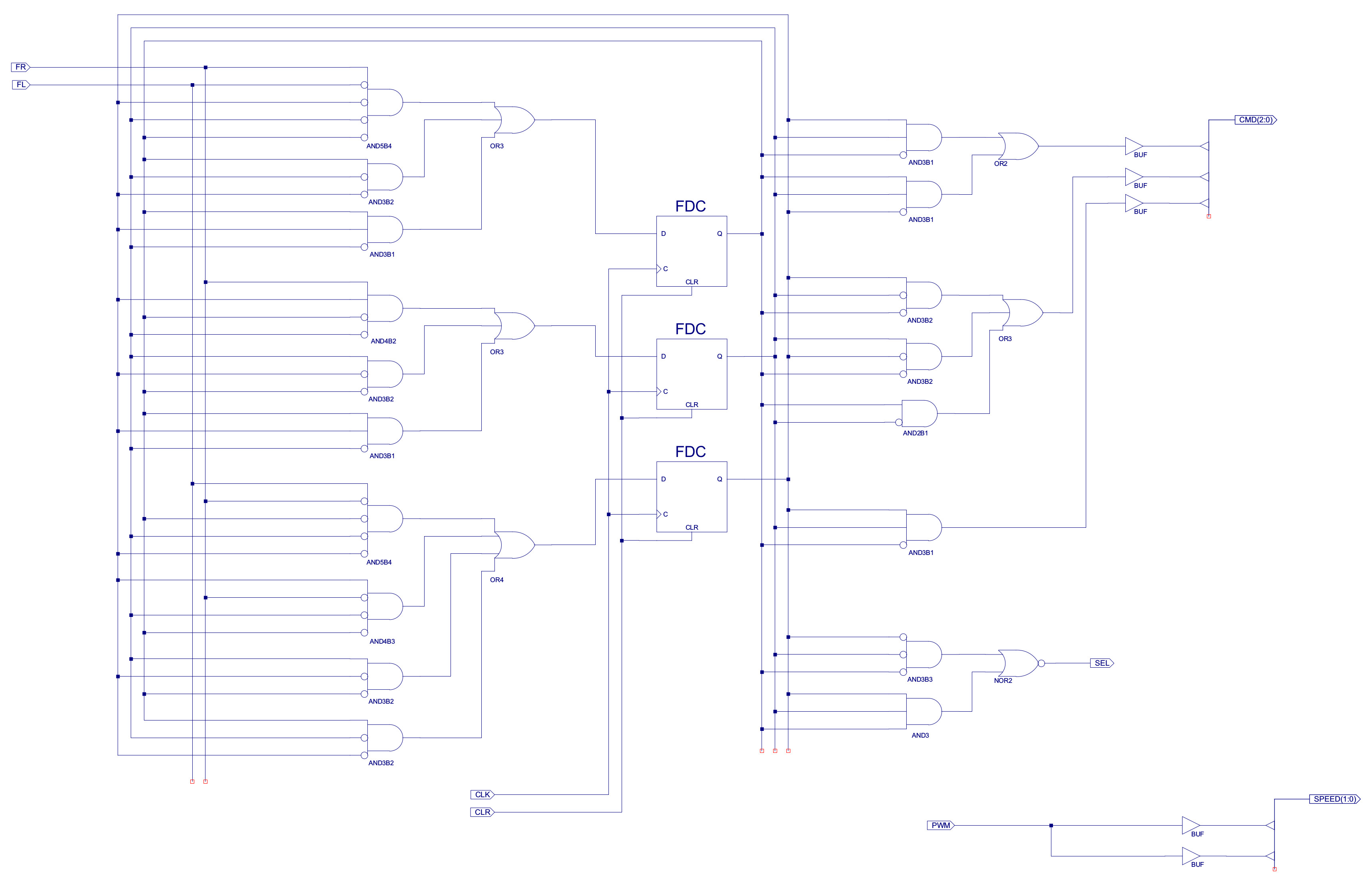
Figure 42 : avoid obstacle circuit diagram
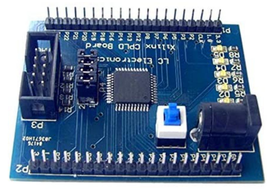
Figure 43 : CPLD
We have now completed the behaviour control network that will be used to implement the cockroach's brain: explore, follow light and avoid obstacle. These state machines will be implemented using a Xilinx XC9572XL complex programmable logic device (CPLD), as shown in figure 43. This programmable hardware is comparable to the FPGA boards used in the labs and can be configured using the same Xilinx ISE software package. CPLDs typically have less configurable hardware elements than FPGAs e.g. this CPLD only has 72 flip-flops, but they are a lot cheaper and do not loose their configuration when turned off. For more technical information on this device refer to: (Link).
You can purchase this board for approximately £7 from your online supplier of choice: Amazon, Ebay, Aliexpress etc. To program this board you do need an additional USB download cable, but we have these in the lab. If you would like, you can also buy one of these cables, however, as the CPLD does not loose its configuration once programmed you should not need this cable again.
The CPLD board will be used to implement the robots brain. We will be looking at the actuator, sensor and power systems in the following sections. Like the FPGA board used in the lab this CPLD can be configured using schematic entry, my top level schematic is shown in figure 44, an almost a one-for-one direct implementation of the block diagram shown in figure 45.
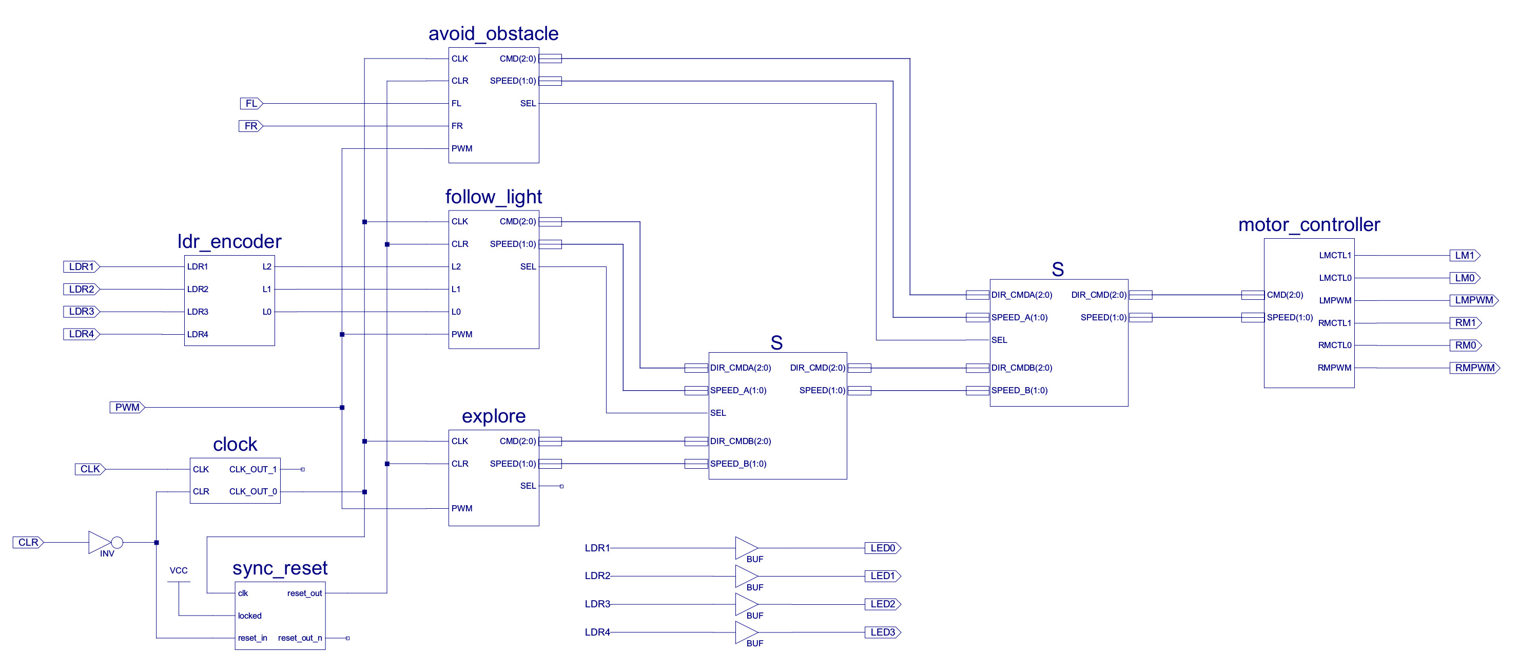
Figure 44 : subsumption architecture schematic
Figure 45 : subsumption architecture block diagram
There are a few of small modifications to the original design:
Task: the joy of using this CPLD is that there is still space / IO pins available to make improvements, add new functionality to the robot i.e. give your robot its own personality :). Improve my design, possible additions could be:
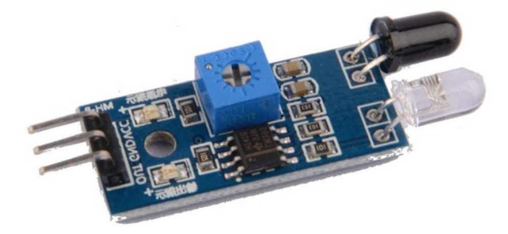
Figure 46 : infra-red sensor
The CPLD can implement the digital circuits needed to control the robot. However, the transistors used in this device are not capable of directly controlling the two drive motors shown in figure 47. The current flowing through these motors is proportional to their load (torque), typically around 10's mA. This current is orders of magnitude more than the transistors in the CPLD can switch. If you were to connect these motors directly to this IC you would probably damage the device. Therefore, the solution is to use bigger, more powerful transistors i.e. an external motor driver circuit.
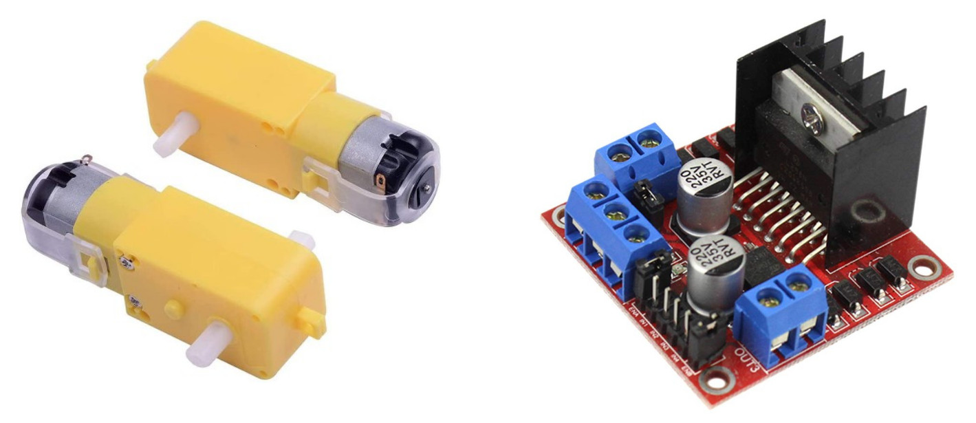
Figure 47 : drive motors (left), L298N motor controller board (right)
The H-bridge motor controller circuit discussed in the actuator section will be implemented using a L298N motor controller IC, shown in figure 48. This IC contains two H-bridge circuits and their associated control logic, therefore, a direct replacement for the circuits designed in the first section. For more information on this IC refer to (Link).
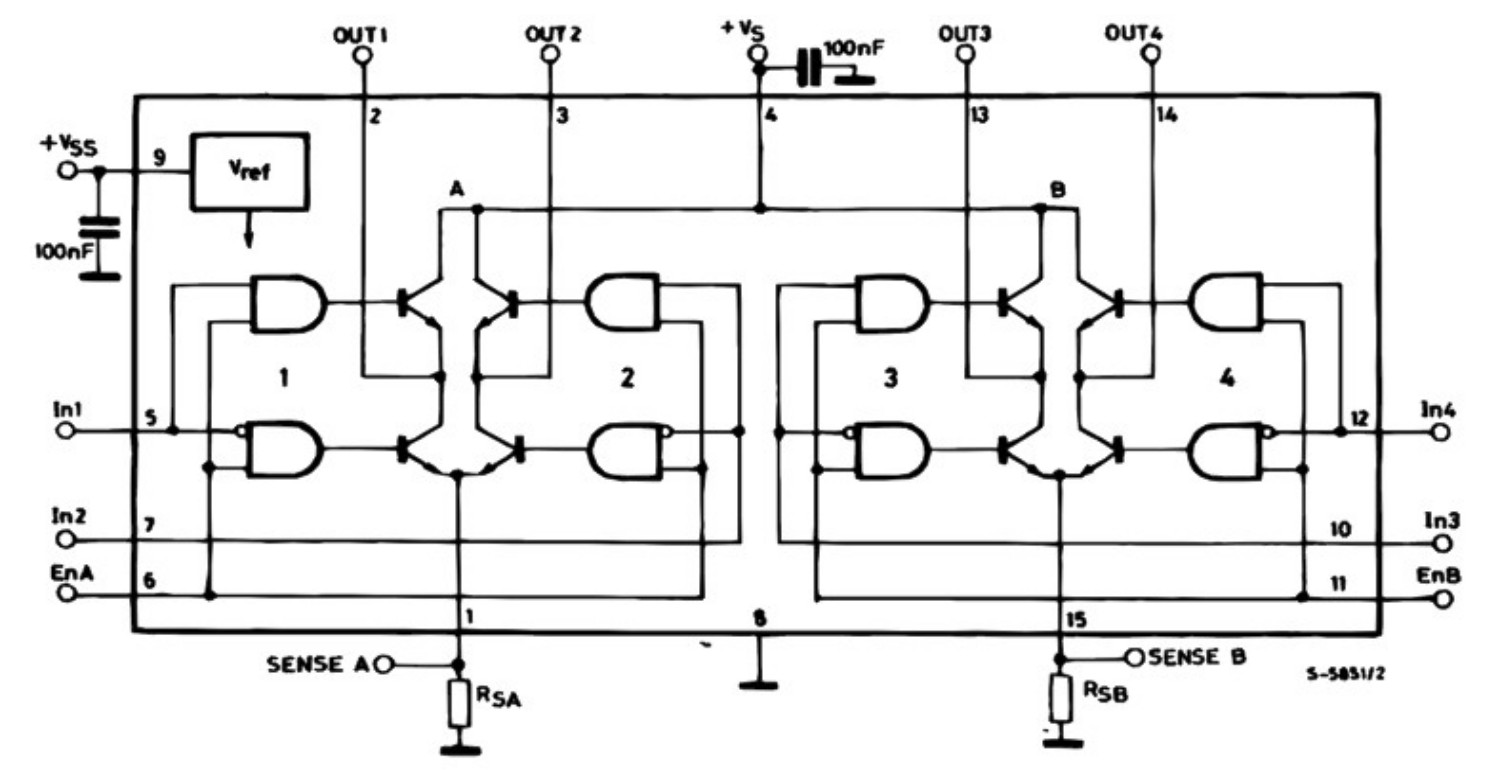
Figure 48 : L298N IC
Each motor is controlled using three signals:
The robot will be powered using a PP3 9V battery. This introduces a small problem, the CPLD needs 5V and the maximum motor voltage is 7V. Fortunately, the L298N motor control board has a 5V linear regulator that will step down the 9V from the battery to the 5V we need. The motor voltage is not actually an issue as you will loose approximately 1V across each drive transistor in the H-bridge i.e. 2V in total. Therefore, the actual voltage seen across the motor is approximately 7V.
You can purchase this board for approximately £2.5 and the motors for £1 each from your online supplier of choice: Amazon, Ebay, Aliexpress etc. For normal usage I would use cheap and cheerful PP3 batteries from your preferred pound store. However, if you want to do a lot of testing then its probably better to buy a NiMH rechargeable 9V battery. These are more expensive, typically around £4, but can have better current outputs i.e. give you more drive power through the motors.
IMPORTANT : power manage is one of the biggest problems for any battery based robot :(. The DC motors used are very effective electrical noise generators, both in terms of radiating electromagnetic interface (EMI) and power supply glitches i.e. spikes and dips on the 0V and 5V supply rails. These problems can causes a lot of issues in practical circuits. One of the most unforgiving and hard to detect are transient glitches on clock lines e.g. 555 timer output. The width of these voltage spikes can be in the nano/micro second time periods, so are very hard to see on an oscilloscope. However, even these short transients can make it seem that your state machines has skipped a state i.e. in reality they haven't, they just interpreted the spike as a clock pulse, skipping through the state diagram in nano seconds, rather than in seconds. Another problem are power surges e.g. when a motor is switched on, resulting in brownouts. This is due to the limitations in battery power. The batteries maximum power is calculated using : Power (W) = Voltage (V) × Current (I) e.g. for the PP3 battery used the maximum voltage is 9V and current is 100mA, so approximately 1W. Therefore, as the battery's power is fixed, if we try take more current than it can provide e.g. robot tries to climb a steep hill, the output voltage will drop. If the battery voltage drops below 7V the 5V regulator on the L298N board will stop working, effectively turning off / resetting the CPLD :(
Solutions: we can add additional power supply filters to help reduce the levels of noise generated from the motors and use better batteries with larger output currents e.g. lithium, but, these problems can still occur, especially when the battery is low on power / discharged.
The previous LDR circuit used to implement the robot's compound eye uses a fixed voltage threshold, however, in a typical scenario we will need to adjust the sensitivity of these sensors to match different background lighting conditions. Therefore, I have modified this circuit as shown in figure 49.
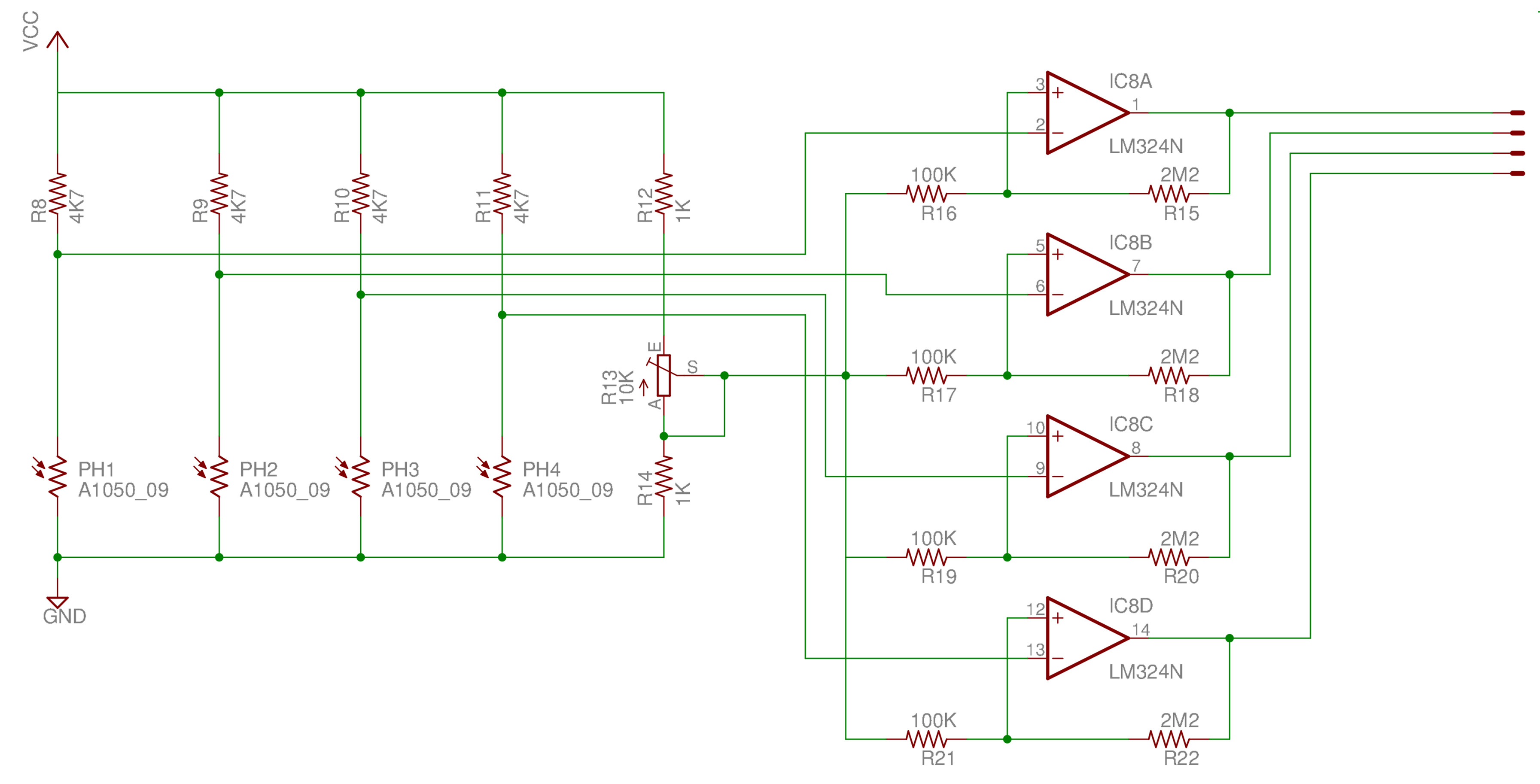
Figure 49 : improved LDR circuit
This circuit uses operational amplifiers as voltage comparators, effectively implementing 1-bit analogue to digital converters (ADC) i.e. if the voltage from the LDR sensor is below a user defined threshold it will output a logic 1, otherwise it will output a logic 0. To adjust the sensitivity of these sensors the user can adjust a variable resistor R13, such that the LDR decode logic produces the DARK (00) output code, then fine tune the sensitivity for the particular destination light source used. For more information on operational amplifiers comparators: (Link).
Note, ideally the CPLD would convert each of these LDR analogue signals into a digital representation e.g. a 5-bit value, representing 32 different light levels. This is possible on the CPLD board using simple RC ADCs, but does add a significant amount of complexity. Alternatively, you could keep the same comparator based system, but replace the variable resistor with a digital to analogue converter (DAC) to allow the system to automatically adjust the reference voltage to suit different background light levels on power up.
The 555 timer circuits (clock and PWM) can also be manually adjusted using variable resistors R2 and R4, allowing fine adjustments of motor speeds etc. The complete sensor circuit diagram is shown in figure 50.
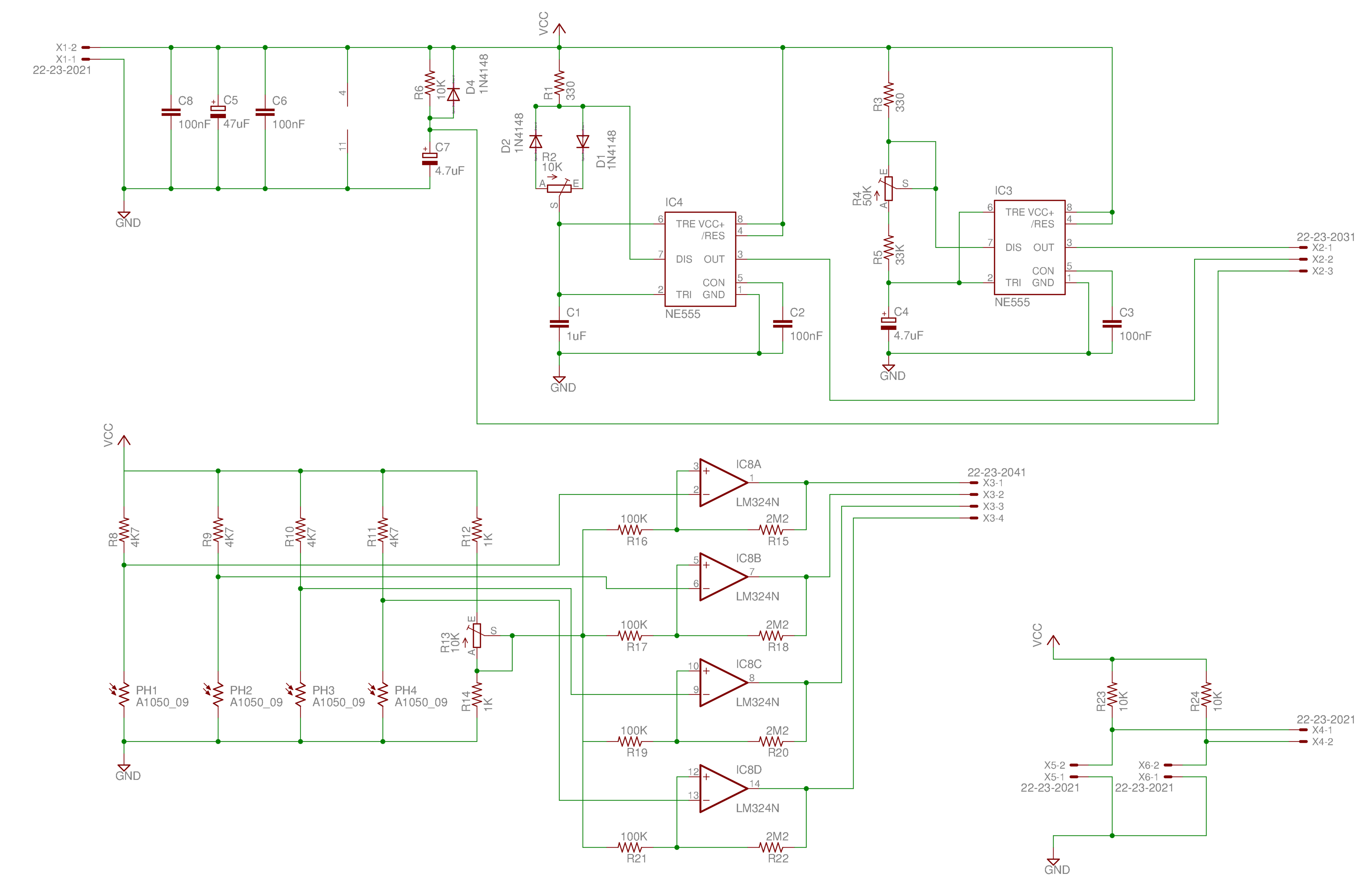
Figure 50 : full interface circuit
To prototype this design i first implemented this circuit on vero-board / strip-board. This single sided prototype board allows initial ideas to be tested on the robot, but is significantly larger than a manufactured printed circuit board (PCB). To produce this prototype the schematic drawn in Eagle (Link) is converted into a Protel netlist, then loaded into the VeeCad (Link) layout tools shown in figure 51.
Note, there are a couple of minor differences between this design and final implementation e.g. the LDRs on the final layout are rotated 45 degrees to fit. Also, changed to few component value to those shown in figure 51 i.e. some capacitor and resistor values, to adjust the 555 timer output frequencies.
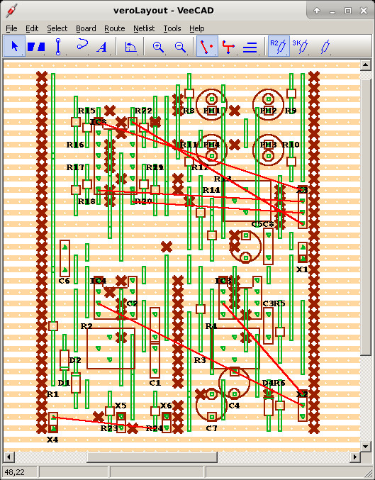
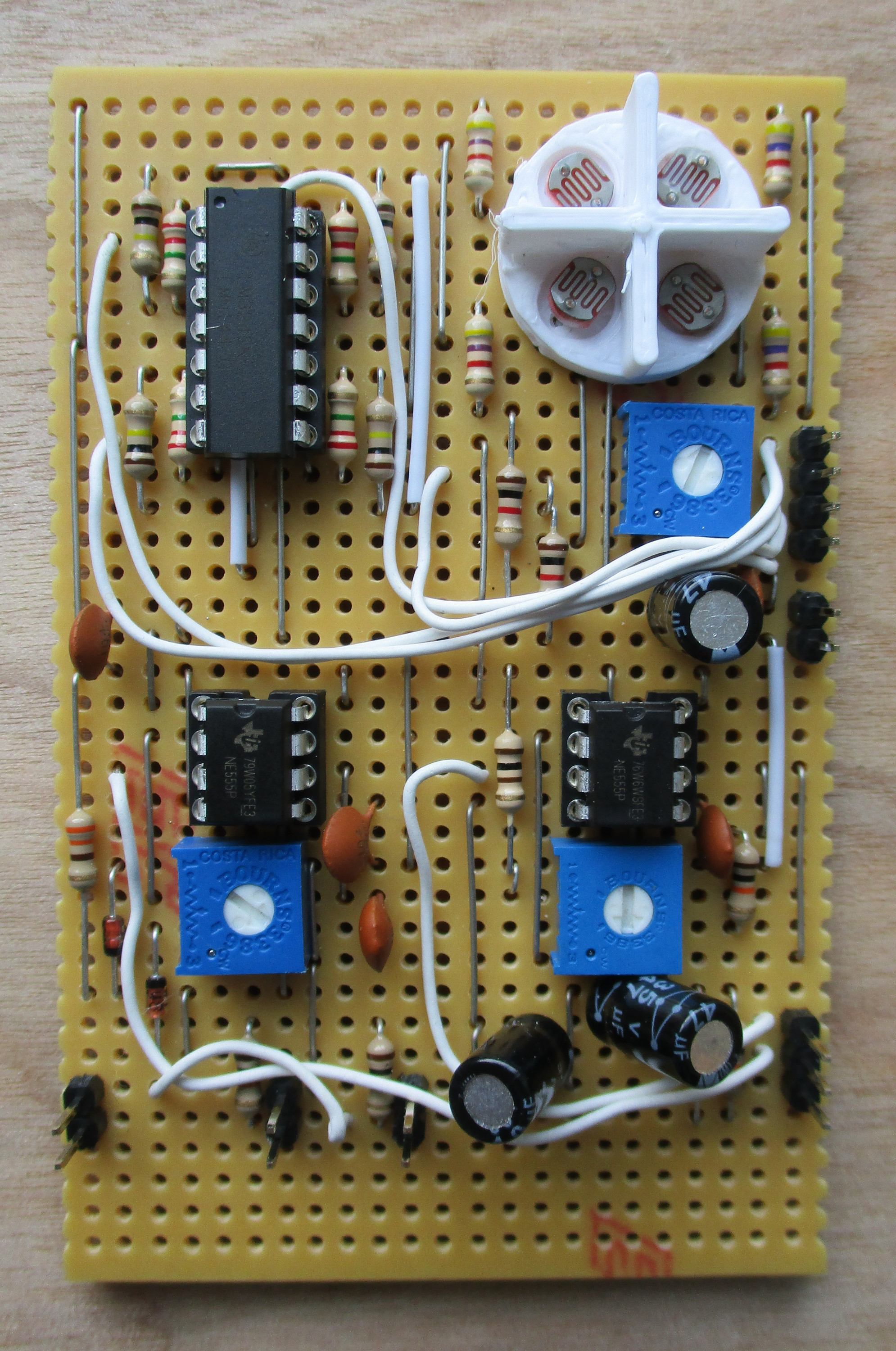
Figure 51 : veroboard layout (left), prototype 1 (right)
A few missed cut tracks and a wire in the wrong place, but apart from that worked ok. Added a reset switch across C7, to discharge the capacitor, to hold the CPLD in reset when powering up / initialising the system. There were a few issues when testing, as expected the circuit suffered from noise problems, to help reduce this i added an extra 100nF + 470nF capacitor pairs across each 555 timer's power rails (big orange, small yellow caps in figure 52), which seemed to do the job. However, as the battery discharges you do see instability / random behaviour as its starts to fade out i.e. the battery enters the last stage of the discharge curve. The various design file are available here:
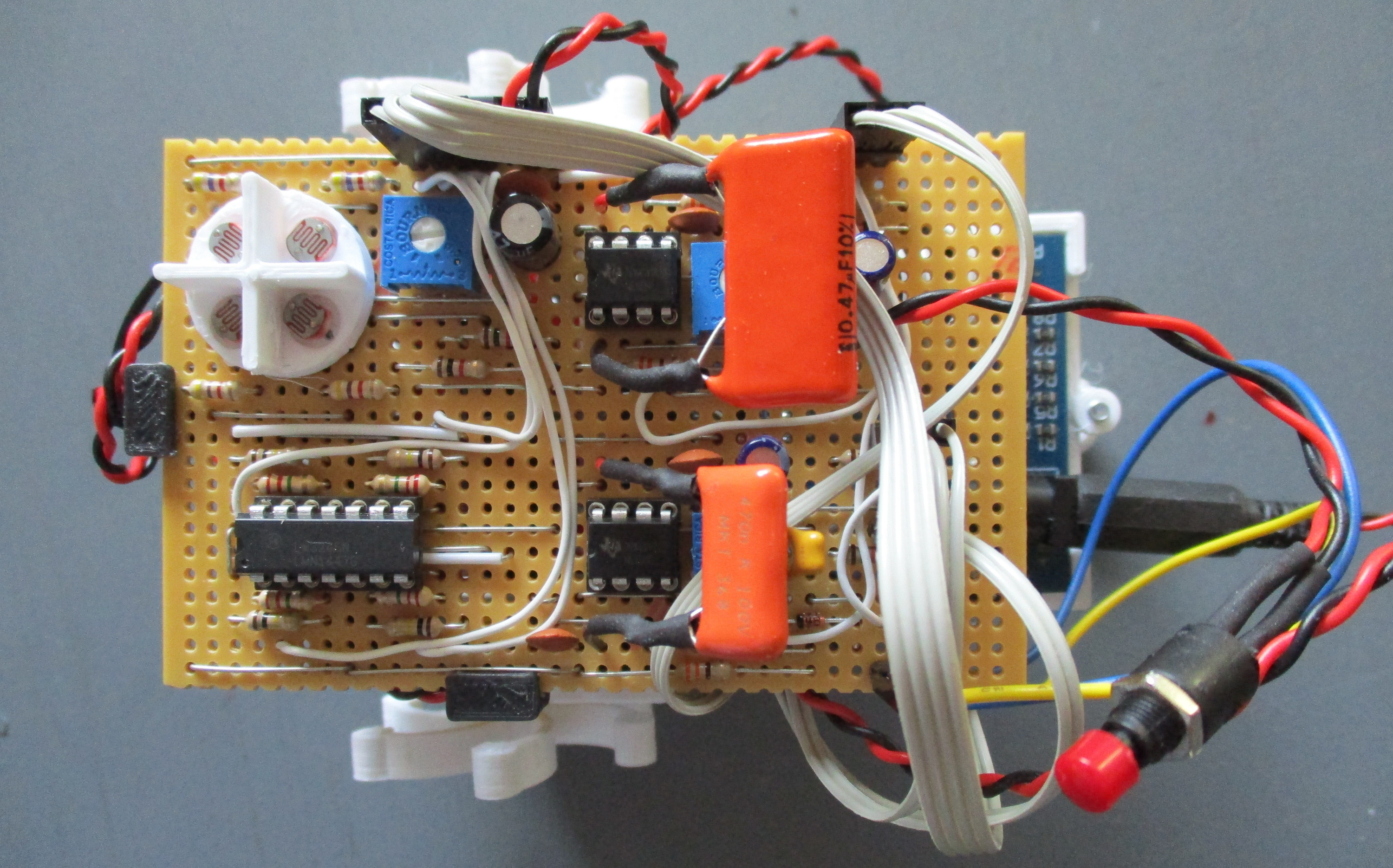
Figure 52 : prototype 1, extra filter caps (orange) and reset switch (red)
As an alternative solution if you do not need the robot to follow light this board can be removed. The system clock and PWM generators can be implemented in the CPLD using equivalent digital circuits, shown in figure 53.
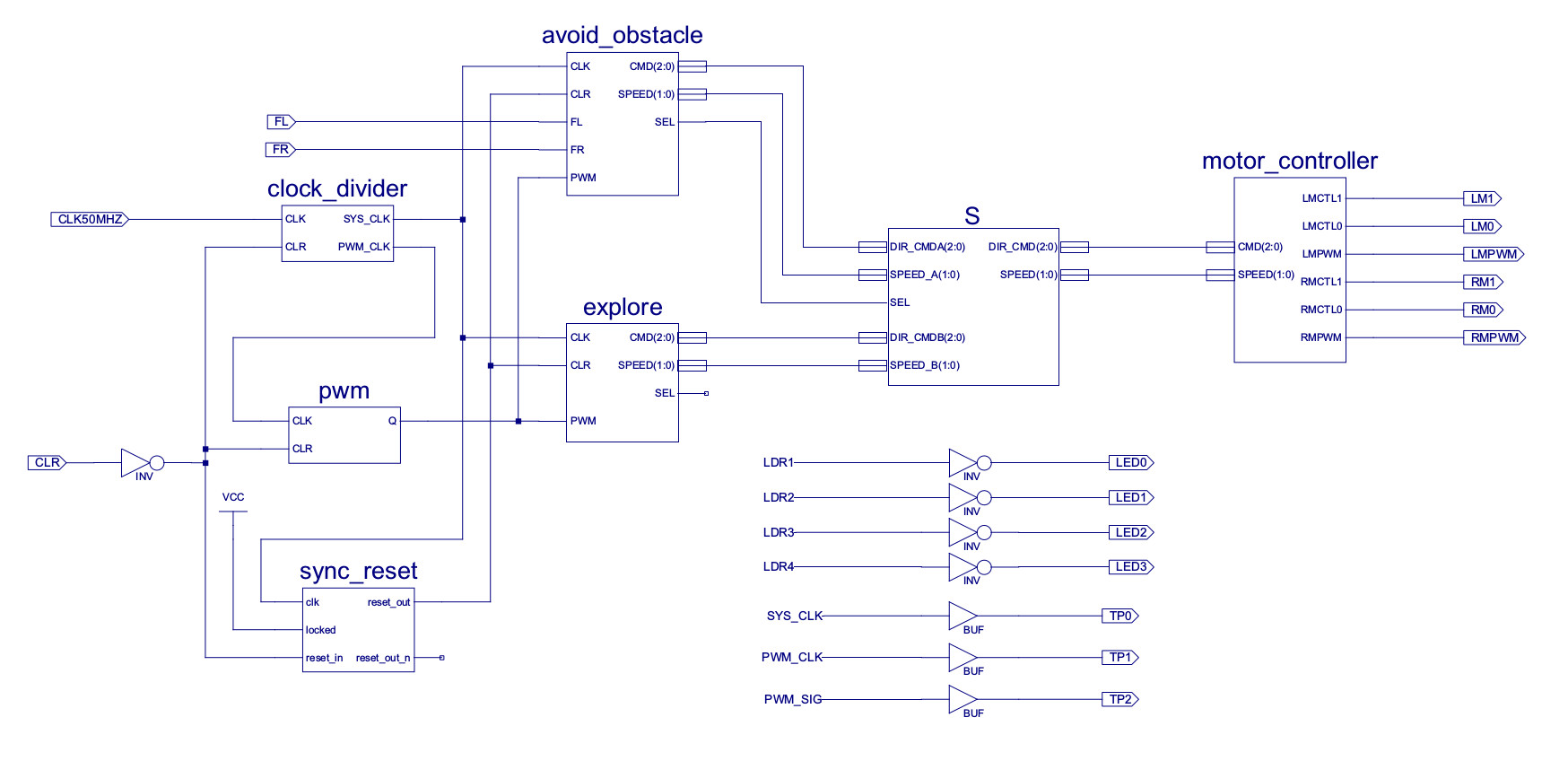
Figure 53 : prototype 2 - CPLD only design
This solution uses the 50MHz onboard oscillator. Therefore, to produce the required 1Hz signal we need to divide this down using a binary counter i.e. each bit from the counter divides the original clock by two, as shown in the simulation in figure 54. The input clock is C, count bit0 divides this signal by 2, bit1 by 4, bit2 by 8 etc.
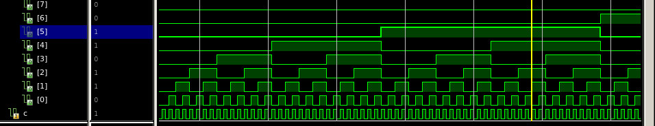
Figure 54 : clock divider
This counter is made from two 16bit counters from the Xilinx component library, as shown in figure 55. These counters are designed to be cascaded to produce larger counts i.e. the clock enable out (CEO) from the first counter enables the second counter for one clock cycle every 2^16 clock pulse. Therefore, together they form 32bit counter. To get a 1Hz clock we need to divide the 50MHz clock by 50,000,000 which is approximately 2^24 i.e. bit 8 of the second counter. The output from this counter pin was measured on the oscilloscope, coming out at approximately 1.5Hz.
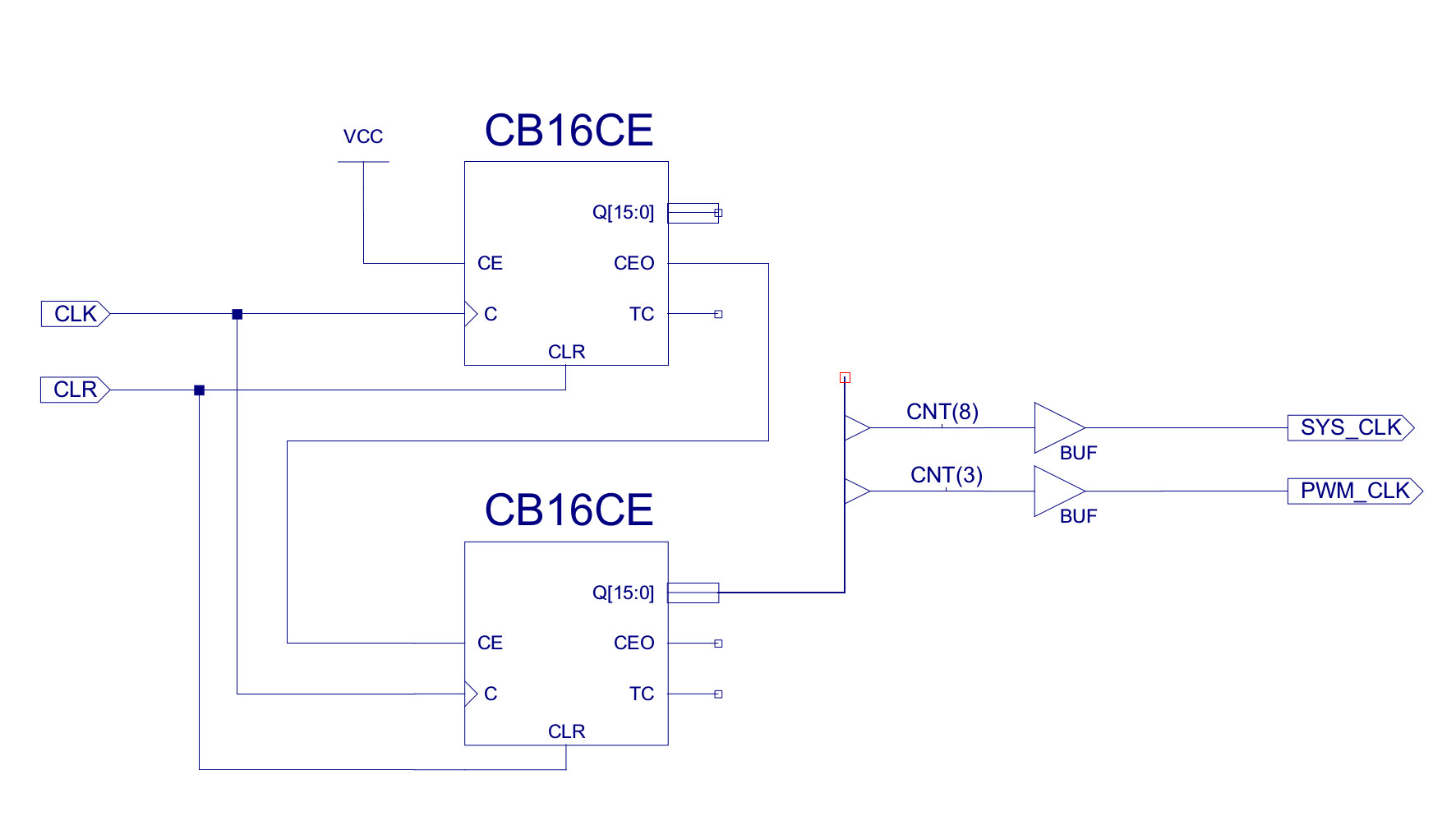
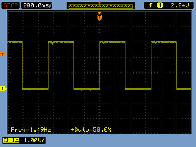
Figure 55 : clock divider
To produce the required PWM signal the ring counter in figure 56 is used. This hardware implements a shift register i.e. the d-type flip-flops are connected in series, with the output of the last flip-flop looped back to the start. Initially on reset the bit pattern 1000 is loaded into these flip-flops, then on each follow clock pulse this bit pattern is shifted right, before finally looping back to the start:
As the PWM is running at a higher frequency than the main system clock, this hardware uses clock divider bit-3 of the second 16-bit counter, as shown in figure 55.
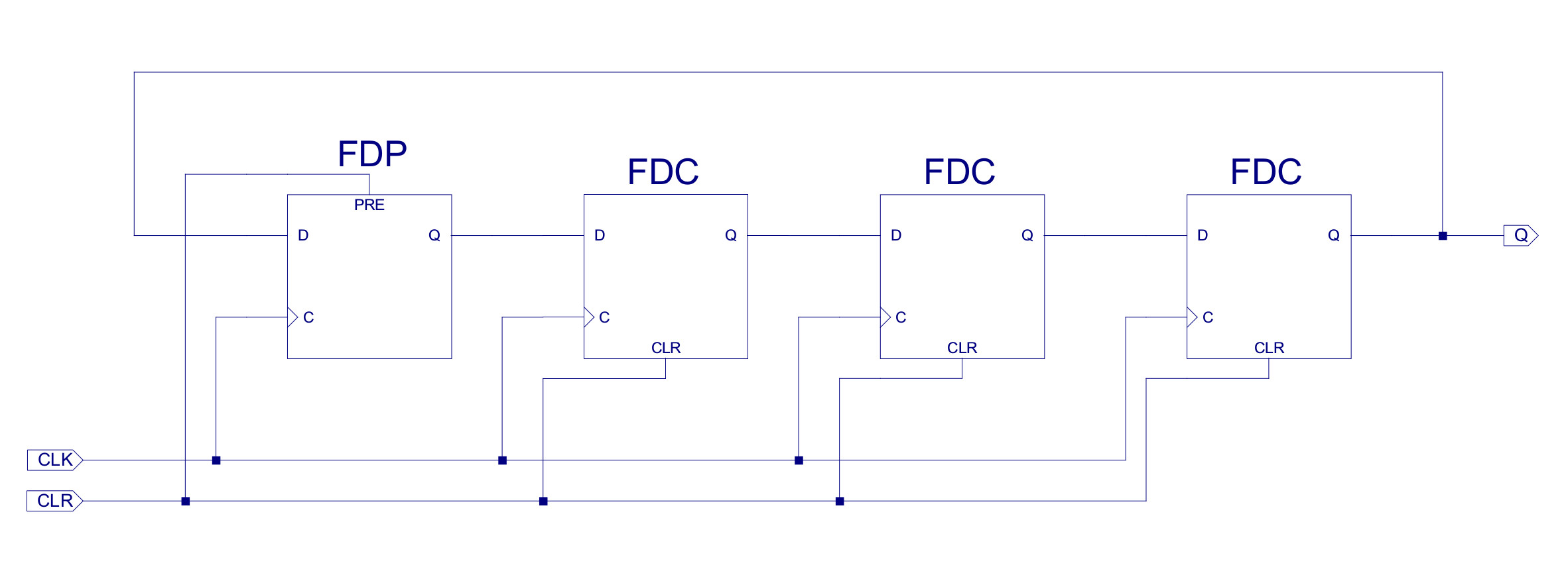
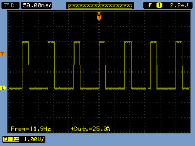
Figure 56 : ring counter
This CPLD only implementation worked fine, the only problem using this approach is the amount of CPLD resources used i.e. you need 24 flip-flop for the binary counter (note, unused outputs from the 32bit counter are automatically pruned by the Xilinx tools) and 4 flip-flops for the ring counter. Thats at least 28 flip-flops from the 72 we have (40%), which significantly reduce the amount of additional functionality / behaviours we could add later.
Figure 57 : chassis parts - base
The chassis is divided into a number of parts to maximise strength, such laminations always run in the correct axis. The parts shown in figure 57 form the base: ladder chassis, battery supports, motor bracket, rear skid and front arms. Mounting points are taped using an M3 drill-tap and joined together using M3 x 6 bolts.
Figure 58 : chassis parts - upper and wheels
The prototype openScad 3D models and STL files are available here:
The first things you learn when using 3D printed parts is that they come with a large amount of clean-up time. I do confess i'm not very good at adjusting the filament settings to minimise stringing etc, so you normally need to use a Stanley knife / small needle file to remove any stringing, lumps and bumps, as shown in figure 59. Use a craft knife to cut off the larger lumps, a sawing action is normally better than force, this helps control the follow through and saves slicing you fingers. Use a needle file to smooth down the inner surfaces. Note, on the motor bracket, make sure you cut and file out the cut-outs for the motor locating pegs (fig 59, left frame). Also make sure you smooth down the back release slope (fig 59, right frame) otherwise you will have problems removing the motors from this bracket.
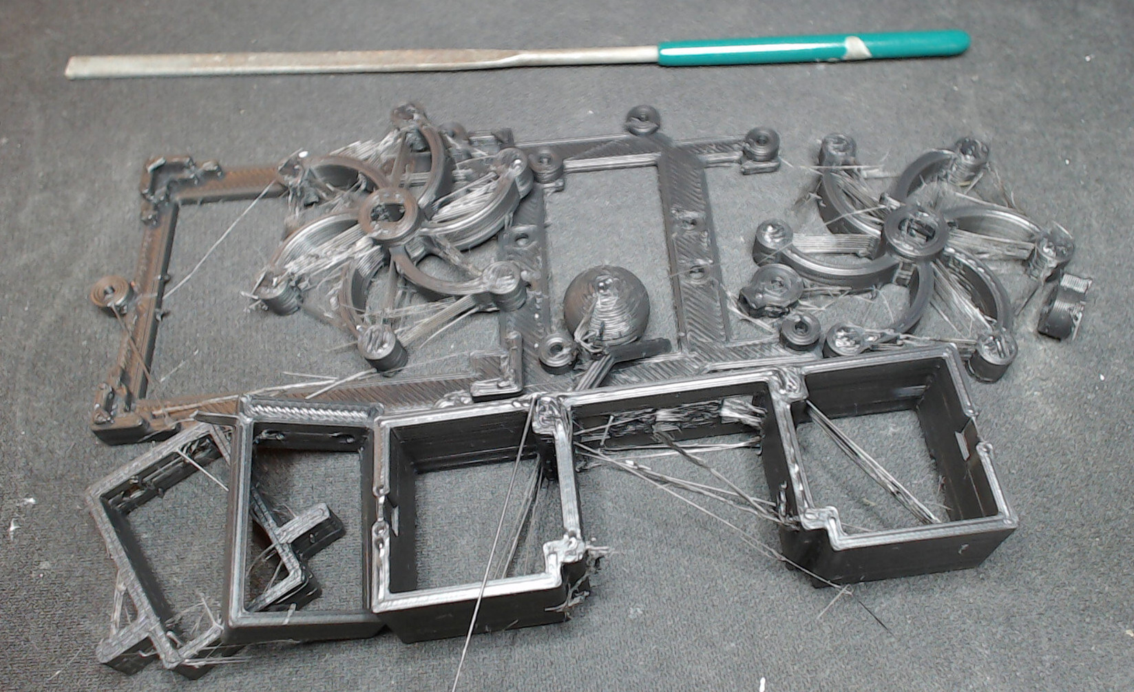
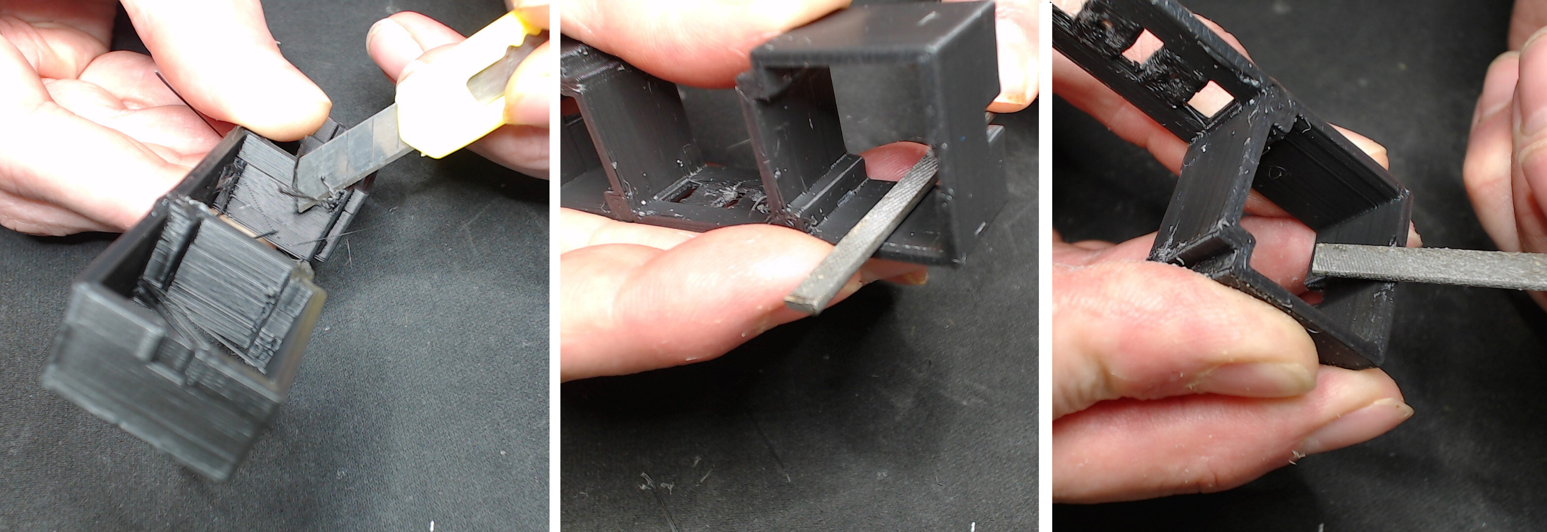
Figure 59 : initial clean up
The wheels are a push / friction fit onto the each drive shaft. Check each hole for any obstructions, smooth inner surfaces using a needle file. If its a tight fit you may need to chamfer the edge of the hole. IMPORTANT, when inserting the drive shaft do no press on the yellow gearbox / case, place the rear of the drive shaft on the table (fig 60, right frame), then using your thumb to push the wheel onto the drive shaft. Test fit, if needed remove and file down the inner surface a little more. IMPORTANT, when removing a wheel you may need to gently, incrementally lever / rock the wheel up the drive shaft.
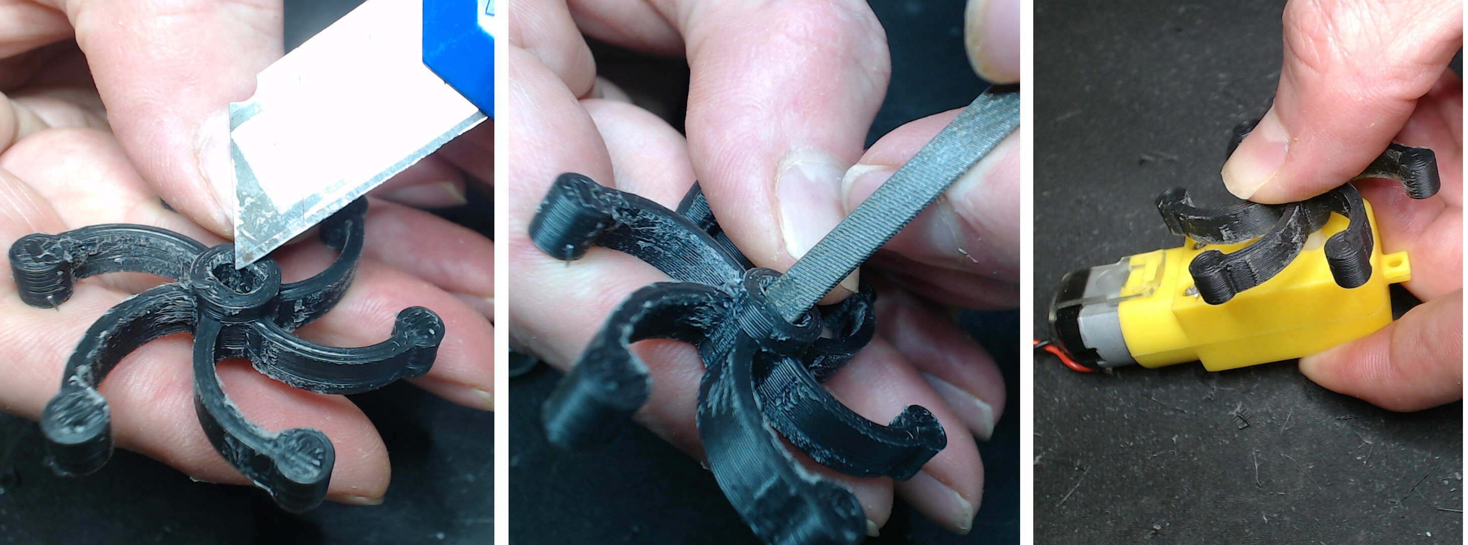
Figure 60 : attaching wheels
Before inserting each motor into the 3D printed bracket, solder wires onto their terminals, do this with the wheels attached (stops motor falling over). Use 13 cm, twisted red and black, 7 strand wire (not single core), as shown in figure 61.
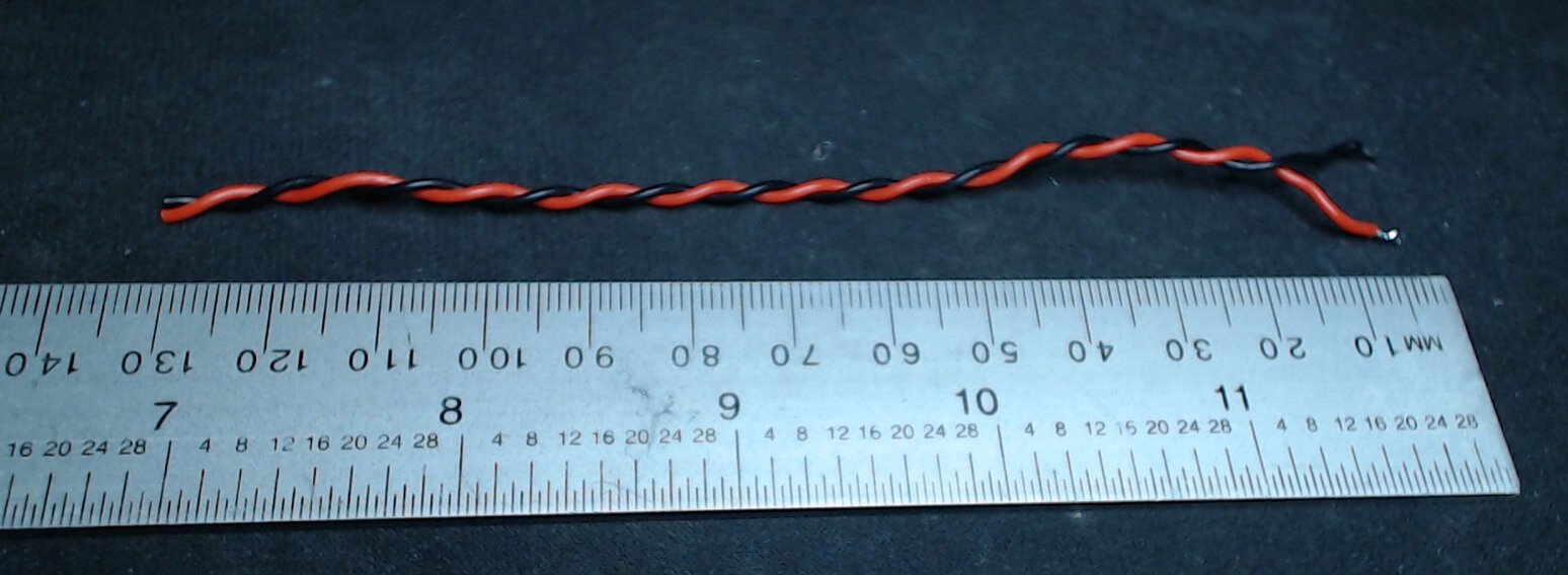
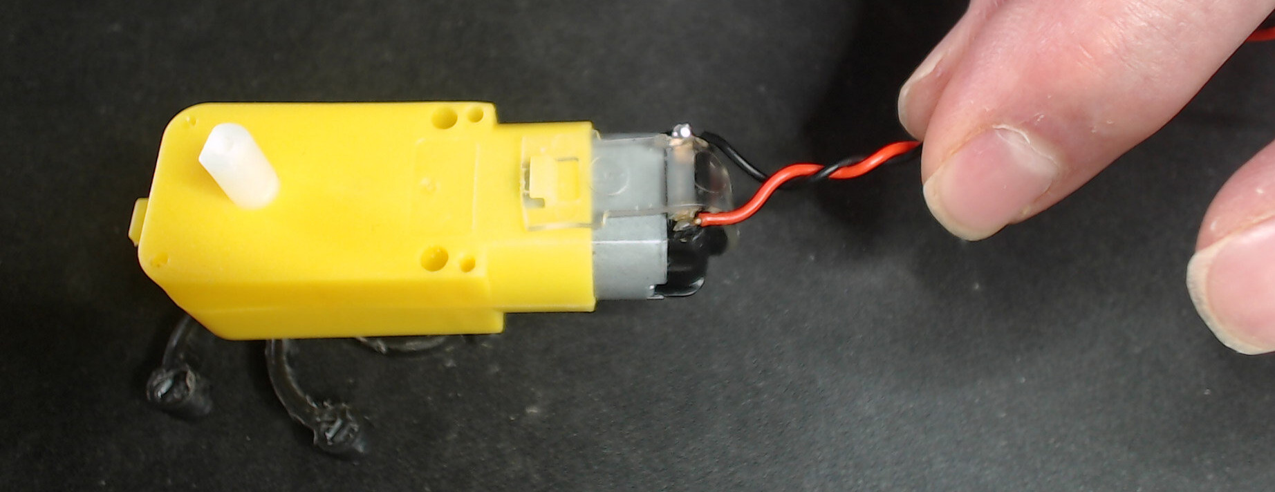
Figure 61 : soldering motor leads and inserting motors
The chassis and battery clips have mounting points that need to be either drilled or tapped, as shown in figure 62, using the M3 drill or M3-drill-tap hand tools. To use these simply insert into the existing 3D printed hole, apply gentle downwards pressure and twist in a clockwise direction. IMPORTANT, when drilling a hole watch out for your fingers and the desk, when tapping a hole make sure you cut threads all the way through the plastic.
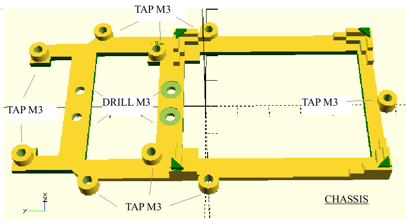
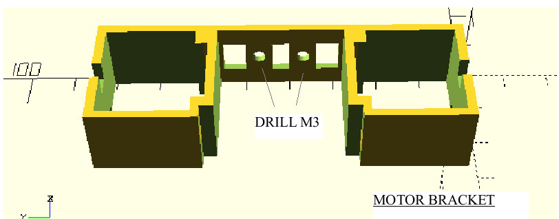
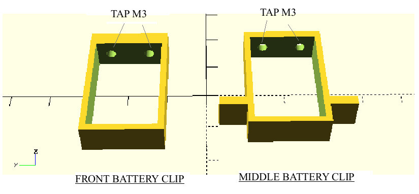
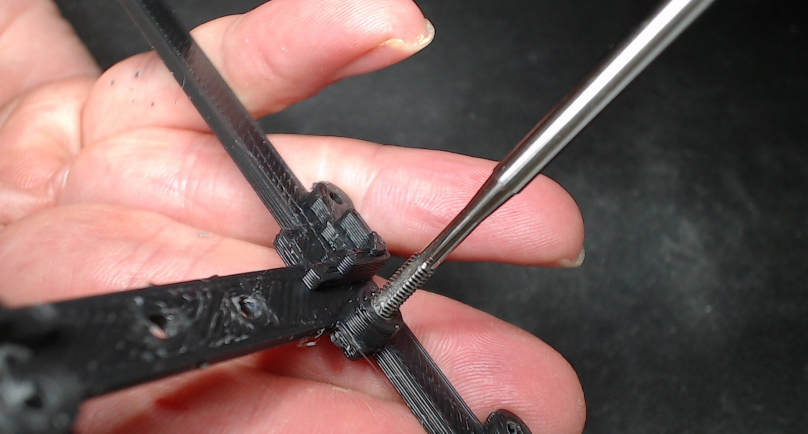
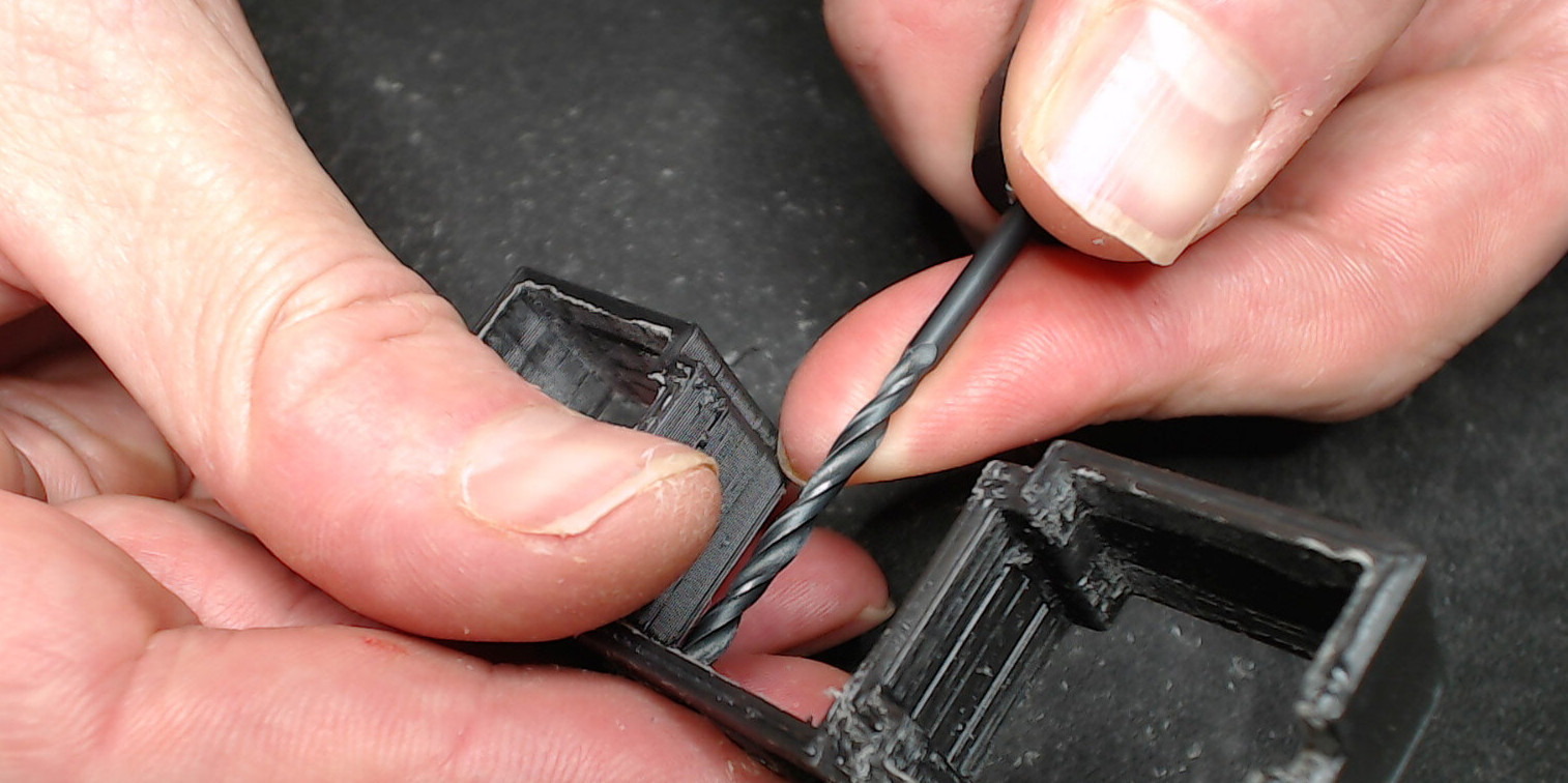
Figure 62 : drilling and tapping holes
Next assemble the chassis, motor bracket and battery clips as shown figure 63. IMPORTANT, make sure surfaces between the chassis, motor bracket and middle battery clip have ALL been filed flat, as these surfaces will be glued together using super glue. Test assemble the pieces using M3 x 6 bolts, as shown in 63, making sure that these surfaces are parallel and flat. Note, super-glue is very good at gluing PLA plastic, but the surfaces must be flat i.e. it will not fill any gaps / voids. IMPORTANT, do not over tighten the M3 bolts, its very easy to strip the threads. If all looks good disable the apply a SMALL amount of super glue on each contact surface between the middle battery clip, motor bracket and chassis. If surfaces are flat, you do need only a small amount of glue. Then bolt (pull) these together using the M3 bolts. Note, the middle bolts are only intended to provided enough clapping force whilst the glue sets, so do not over tighten. IMPORTANT, make sure that the chassis and motor bracket are square before leaving the glue to dry, needs at least 10 minutes, but an hour if possible. Do not glue the front battery clip as you may need to adjust this when inserting the battery.
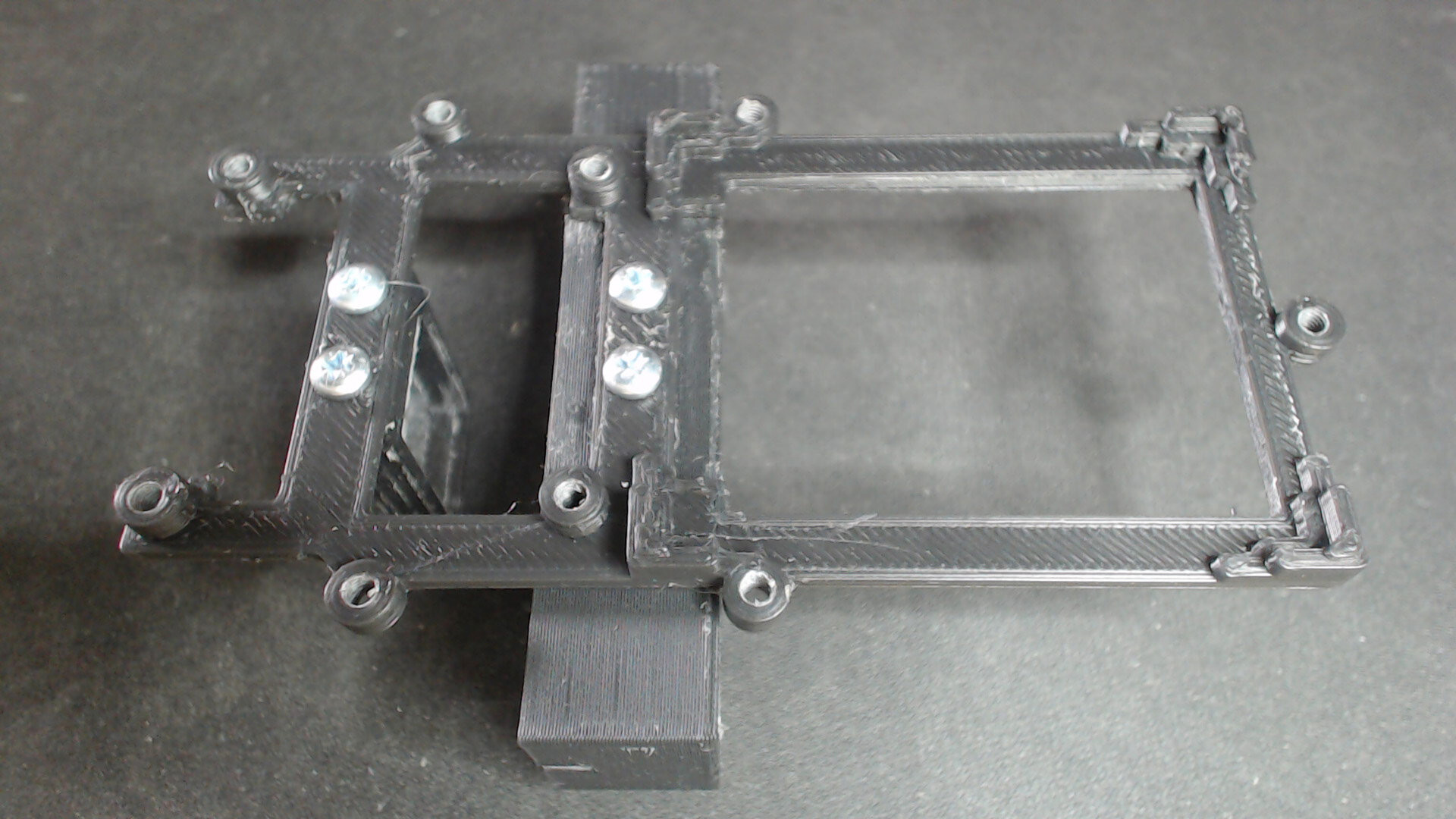
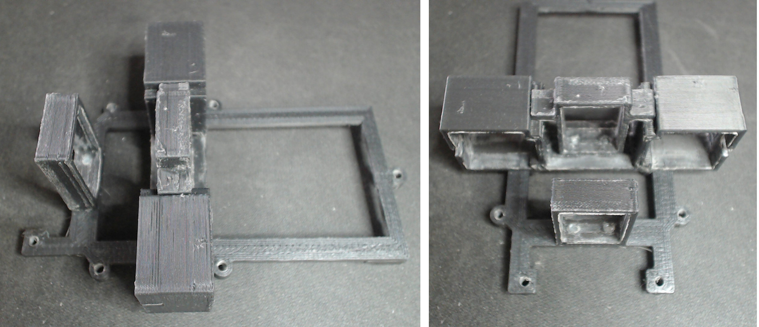
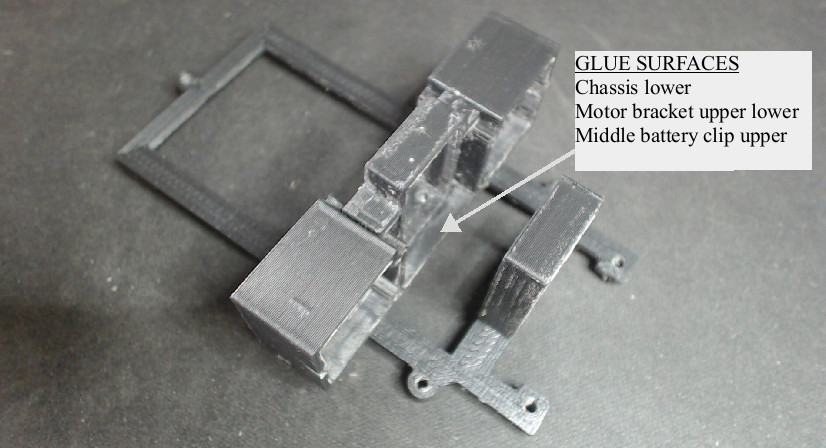
Figure 63 : assembling chassis
Insert each motor into the motor bracket as shown in figure 64, ensure each motor's mounting post slots into the recess and the the wheel "legs" face forwards. Then feed motor wires through the bracket towards the front of the robot.
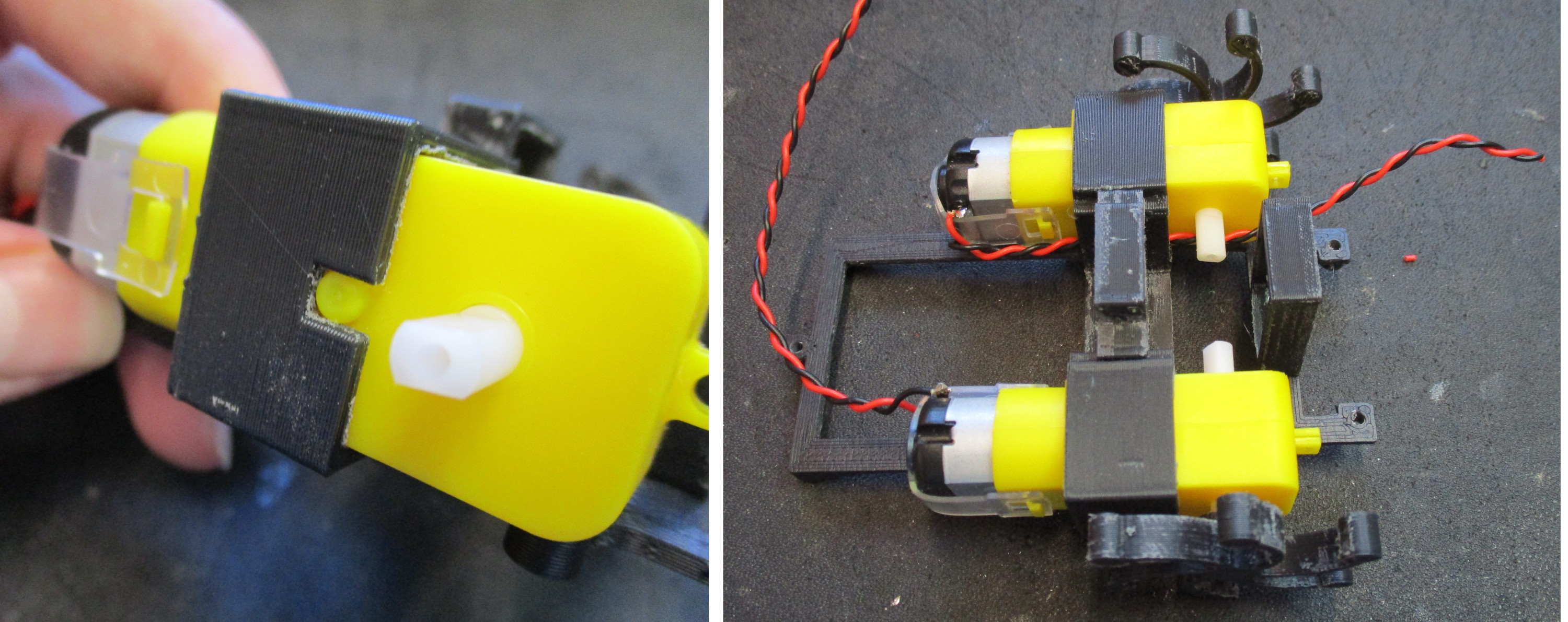
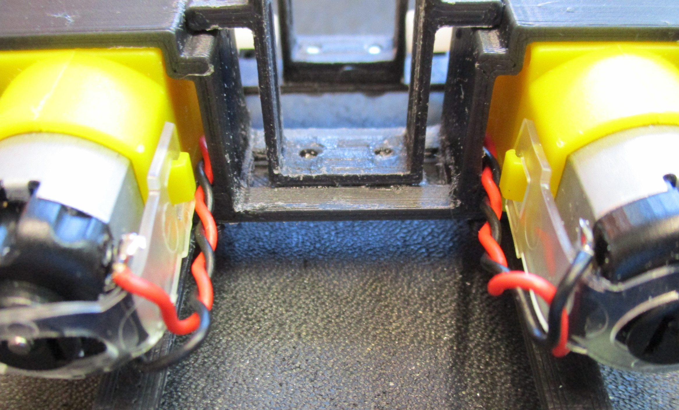
Figure 64 : mounting motors
File down any bumps on the spherical rear skid, then mix-up a small amount of 5min epoxy (a small pea size blob of epoxy and hardener), mix then fill the holes, insert the head of the M3x25 bolt and leave to set, as shown in figure 65.
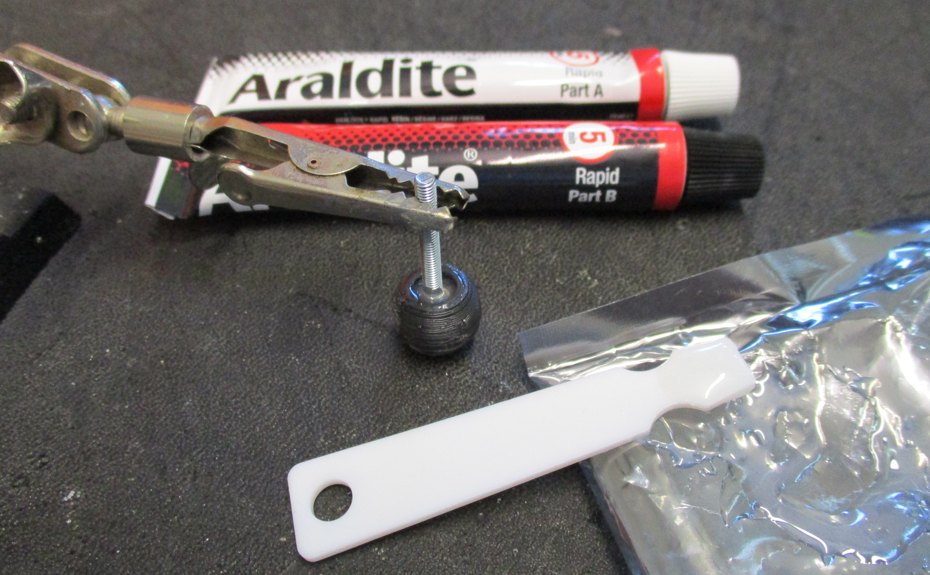
Figure 65 : rear skid
The front motor drive board is attached to the chassis using M3x6 and M3x15 bolts. The shorter 6mm long bolts secure the back to the board, the 15mm bolts the front. Note, the bumper sensor arms also mount onto the front 15mm bolts. The CPLD simply clips into the four corner posts. When dry screw the rear skid into the back mounting post and lock into position with an M3 nut, as shown in figure 65.
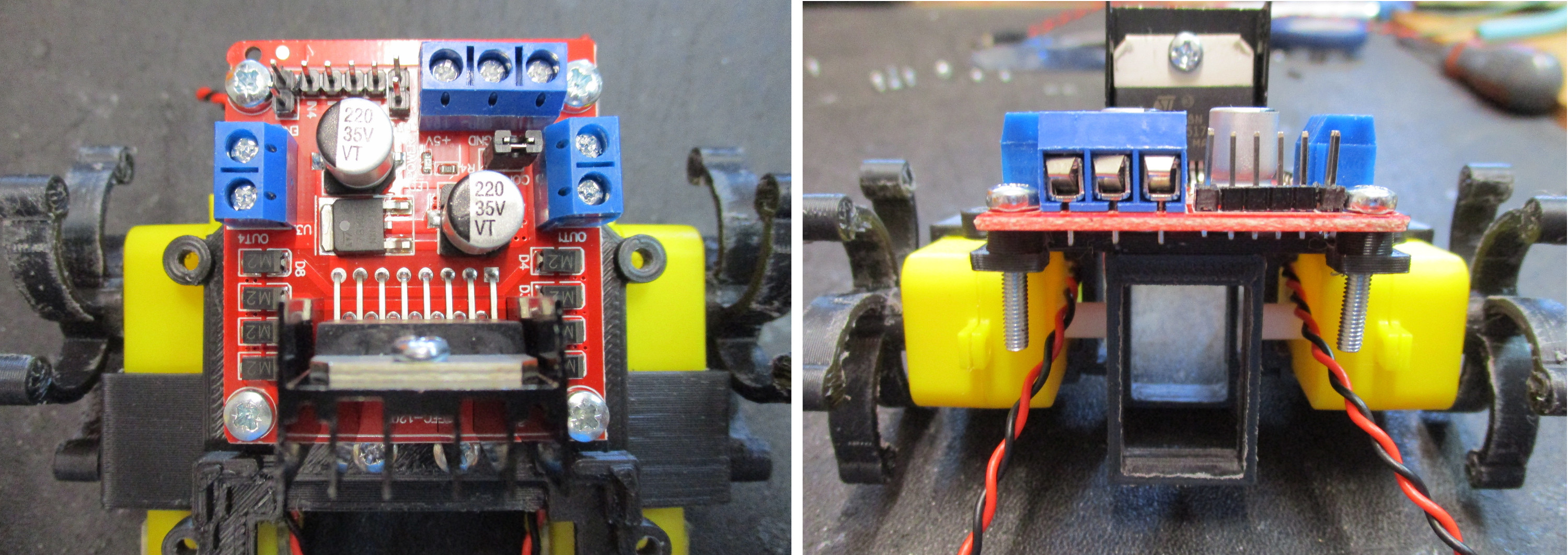
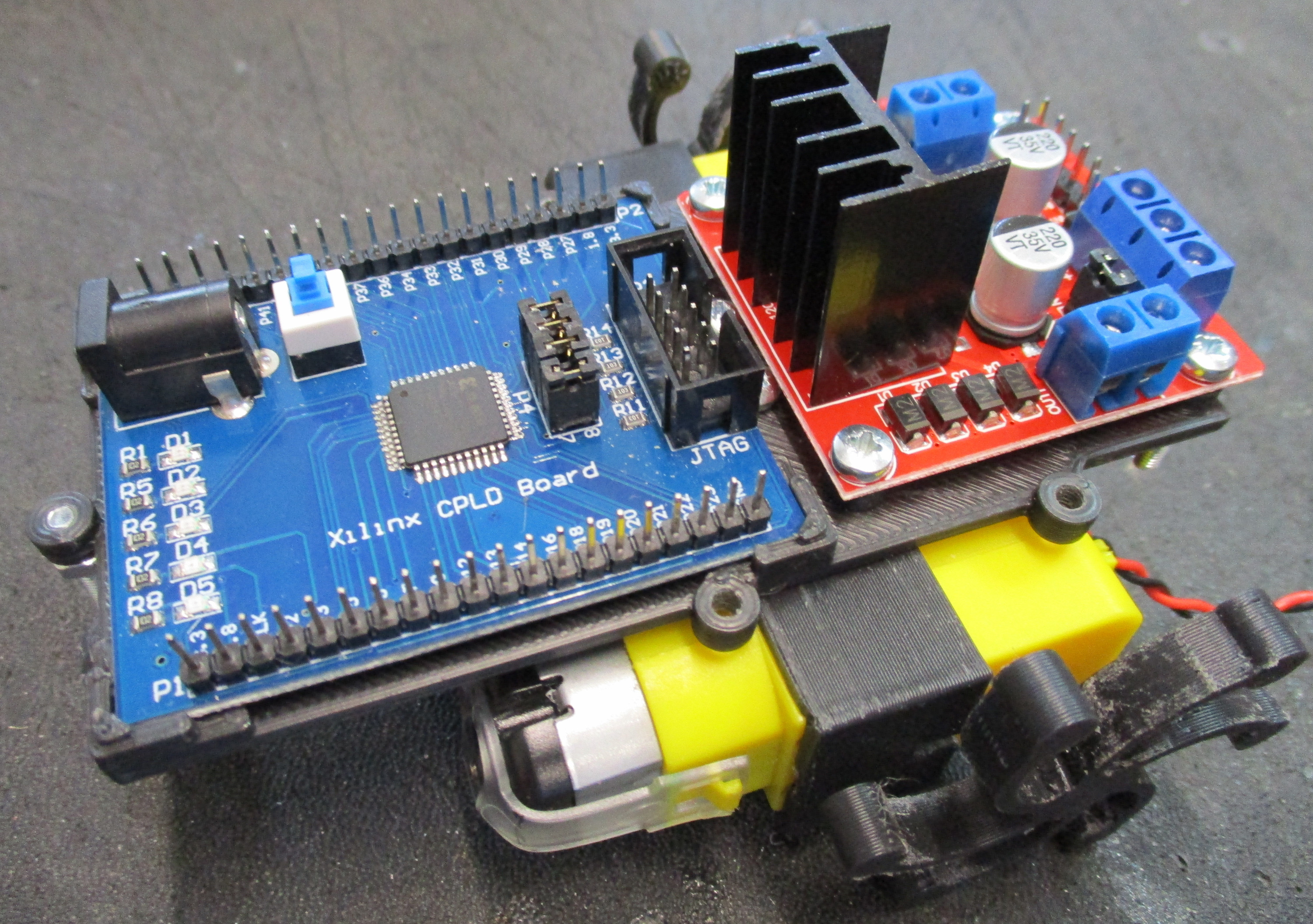
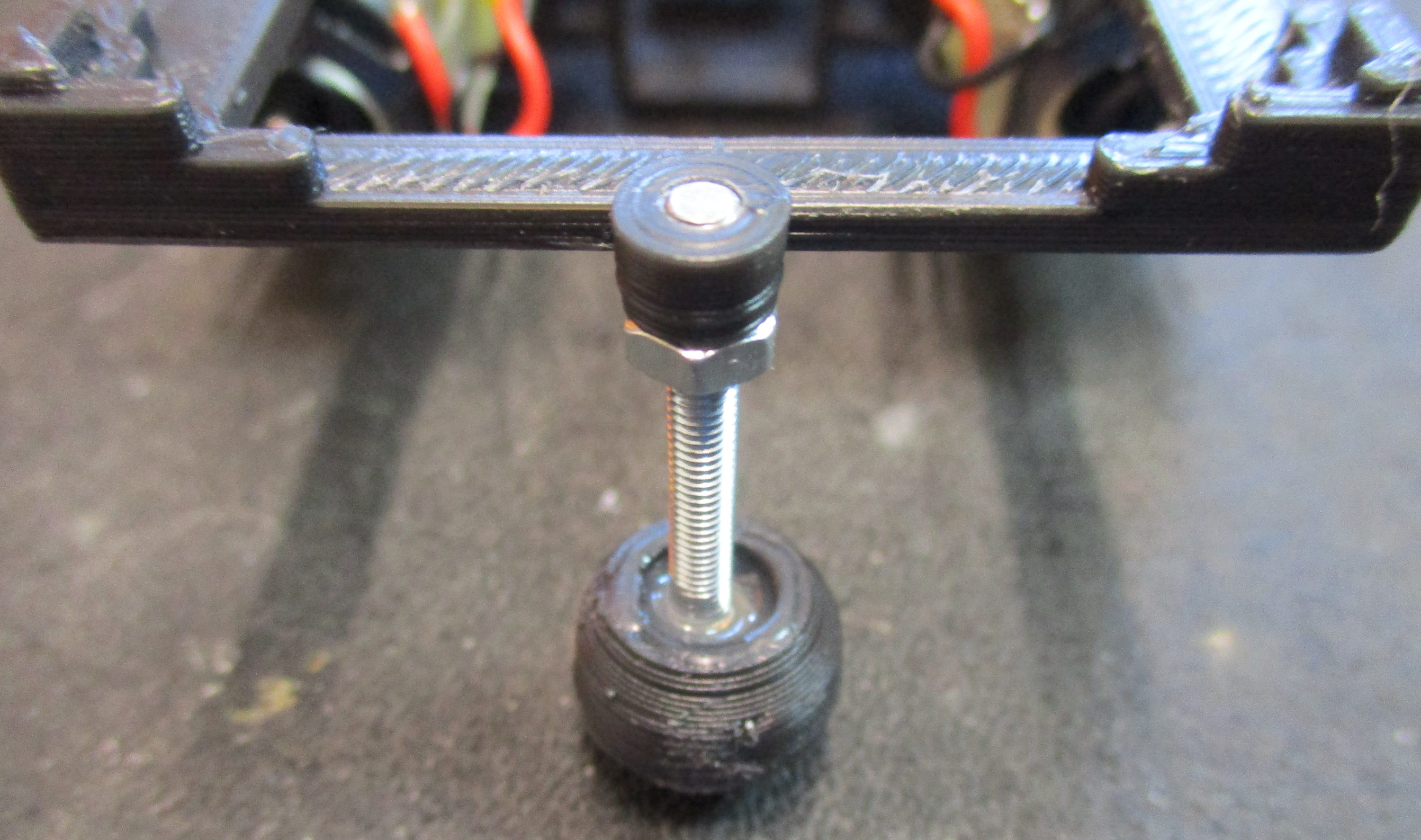
Figure 65 : attaching motor drive and CPLD boards
Cut a 8cm length of single core red wire and a 12cm length of black, strip off insulation, keeping a two 25mm lengths for later, as shown in figure 66. Inset one end of the 8cm length of wire down into the front hole, wrap wire around plastic arm approximately three times and feed the free end through the second hole. Next, feed a 25mm strip of red insulation back onto the wire, leaving a 1cm exposed section at the end, as shown in figure 66.
Insert the 12cm wire up into the third hole, feeding through approximately 6cm, then wrap the back section of wire around plastic arm three times and feed the free end through top hole. Feed a strip of insulation back onto wire, leaving a 1cm exposed section at the end, as shown in figure 66. If needed drill out the arm base using a M3 drill. Test fit the two arm pieces, as shown in figure 66, file flat where needed. Disassemble, place a small drop of super glue into the square hole, insert arm and allow to dry for 10 minutes (half an hour if possible). Then attach to the front M3x15 bolts using a star washer and M3 nut as shown in figure 66.
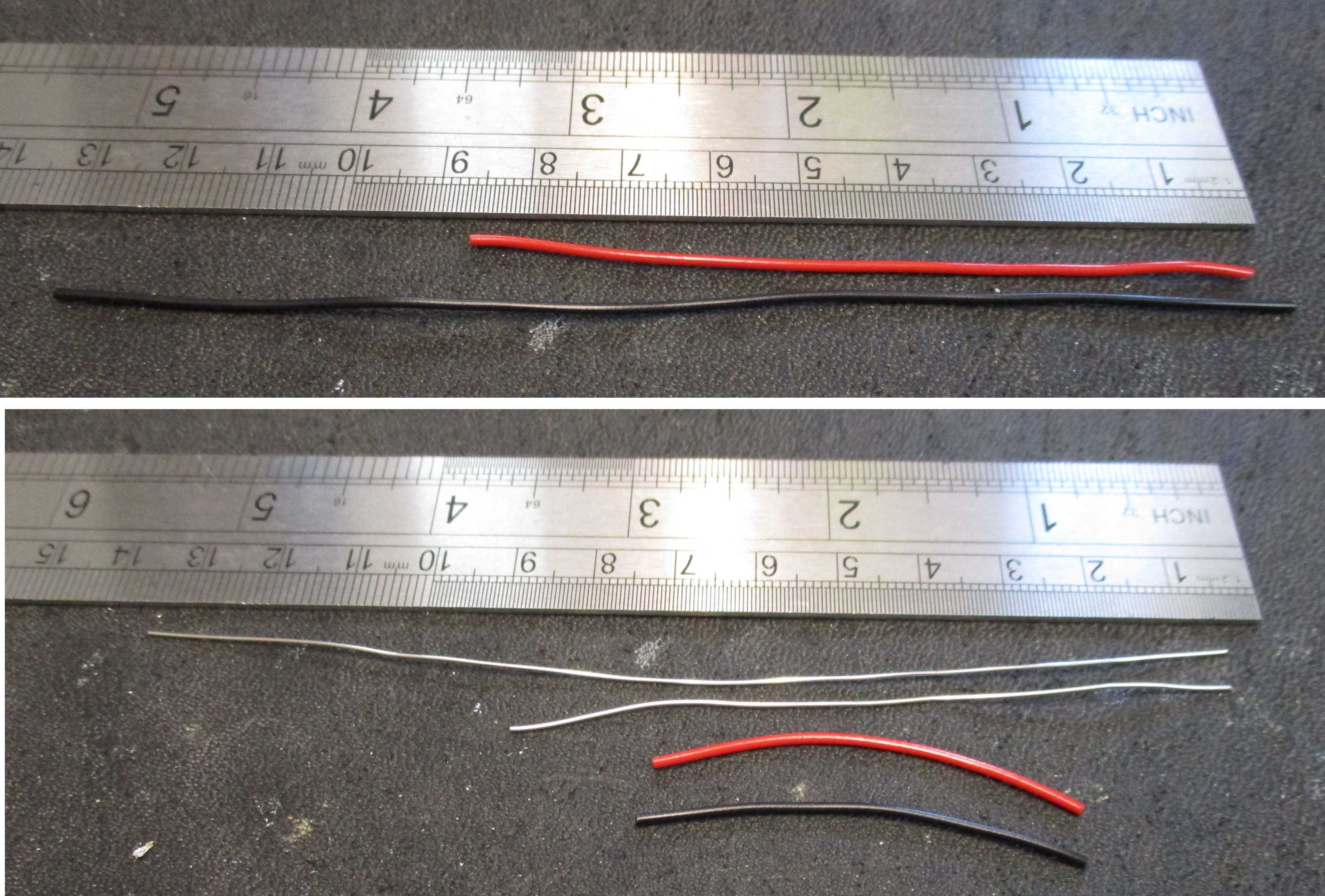
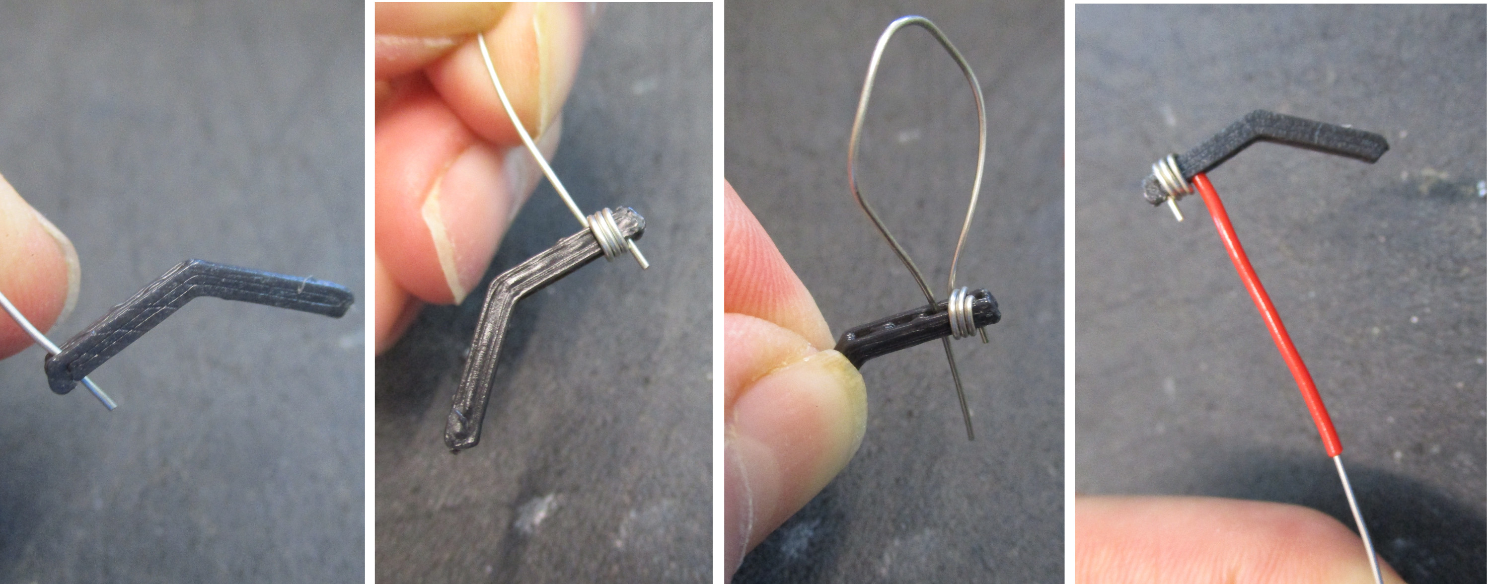
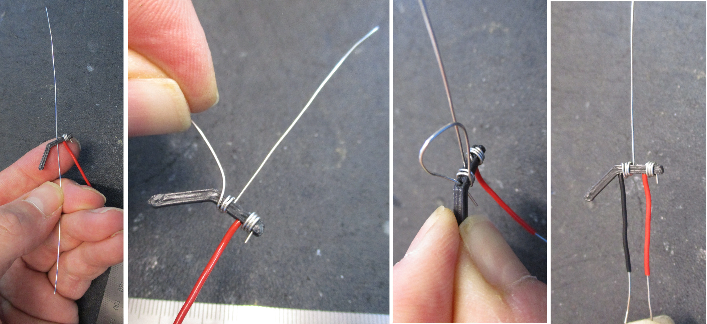
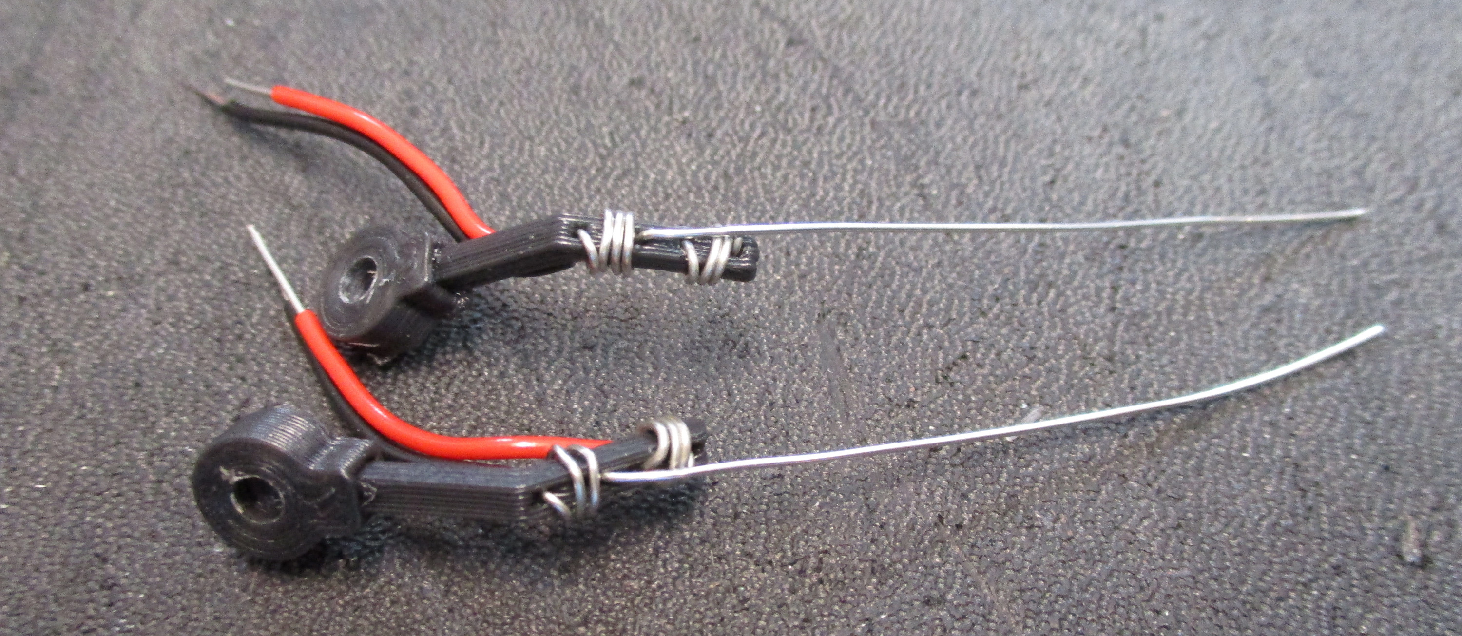
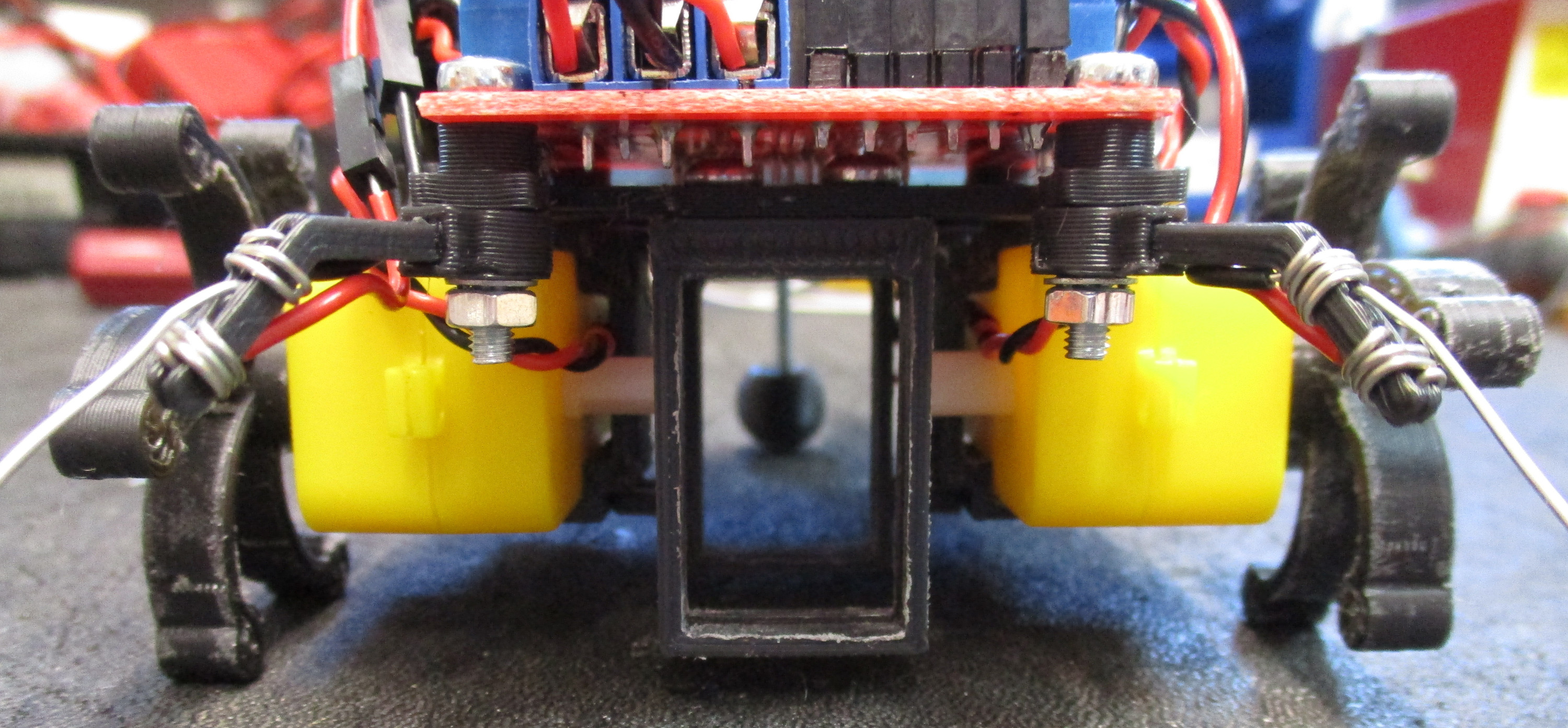
Figure 66 : bumper switch
Cut and strip the motor wires to length, strip off approximately 5mm of insulation to expose the copper wire, twist strands together and insert into motor controller board's side terminal blocks. The PP3 battery clip is wired into the front three-pin terminal block, as shown in figure 67. The 5V output is connected to the CPLD using a 2.1mm plug, wired using a 25cm twisted red and black, 7 strand wire (not single core), centre positive (+5V), outer negative (0V). Note, the all circuit share a common 0V line.
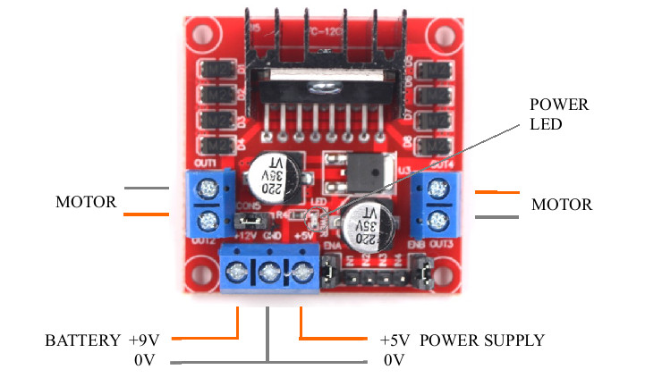
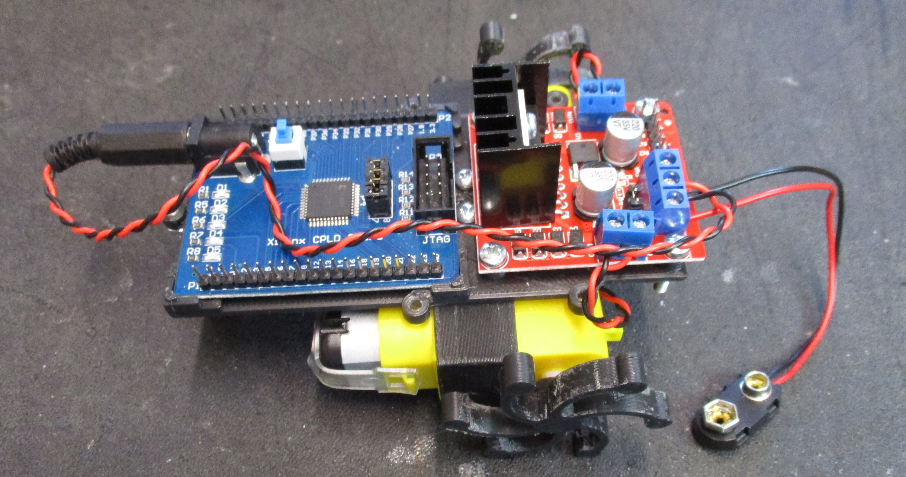
Figure 67 : wiring motor and power supply
The bumper sensor signals and motor control signals are attached to the CPLD board using female-female jumper leads as shown in figure 68. Red and black cables are pushed onto the single core bumper switch wires, then the black leads are plugged into the GND pins on the CPLD, the left switch red wire into pin 37, the right switch red wire into pin 36. The motor control signals are wired as shown below i.e. the orange and yellow wires. Remove the ENA and ENB jumpers, these are the PWM control lines i.e. the green wires. There is also a purple reset wire connect between pins 42 and 27. In this position the robot will be held in a reset state (handy to prevent the robot moving off when being programmed). Moving the lead from pin 27 to the 3.3V pin at the end of the edge connector will enable the robot. Finally, insert the battery into the battery clips, but do not connect the battery connector yet.
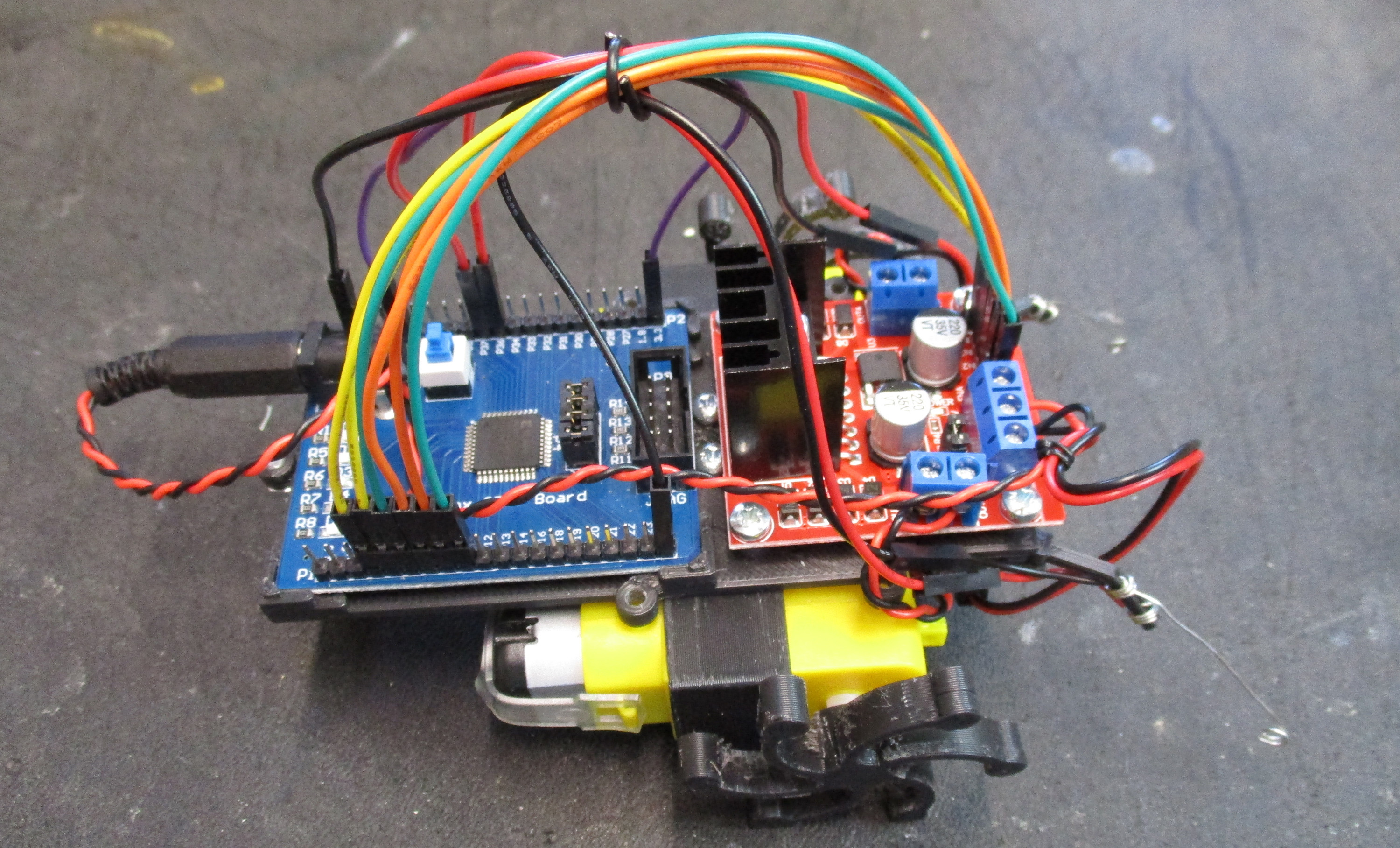
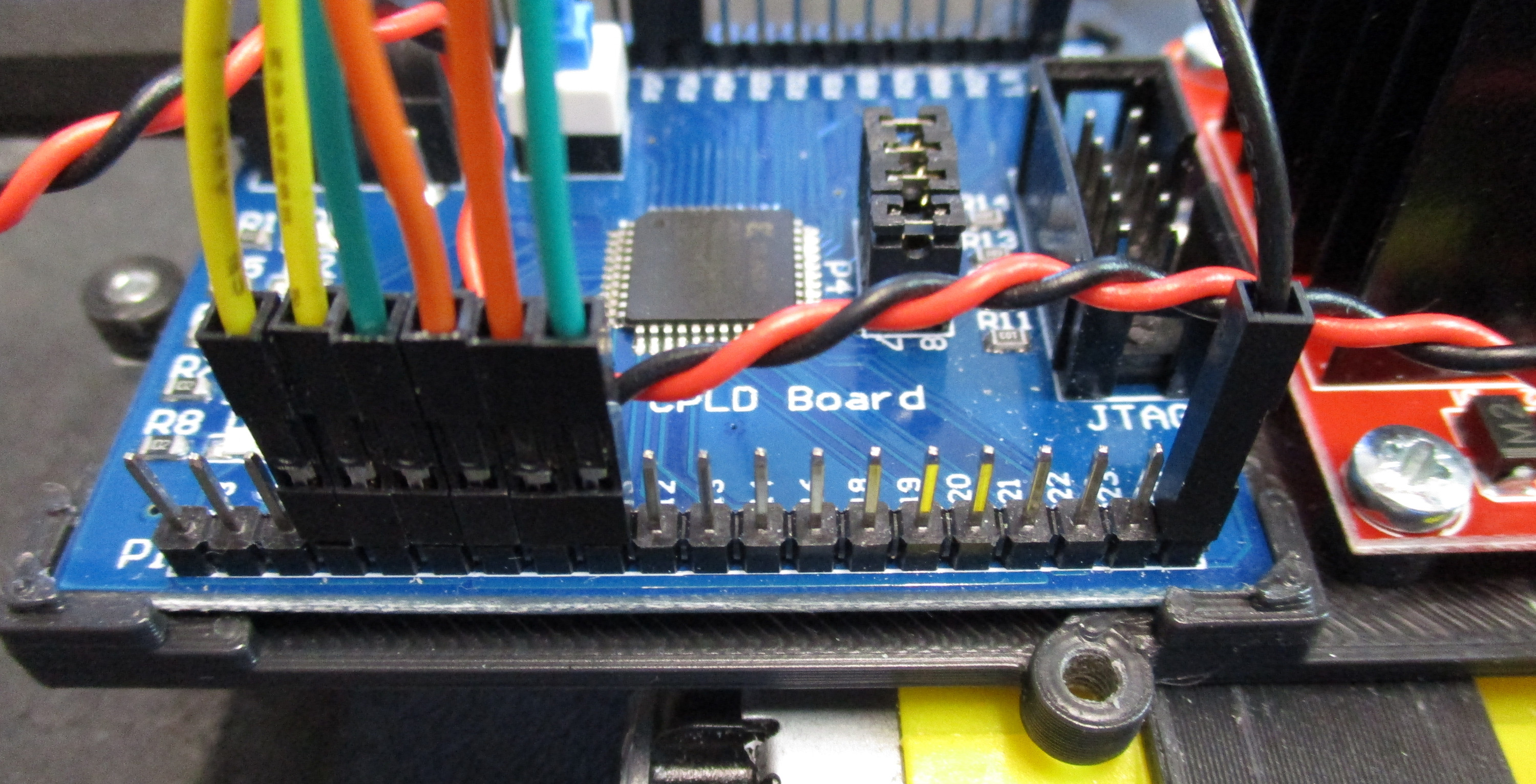
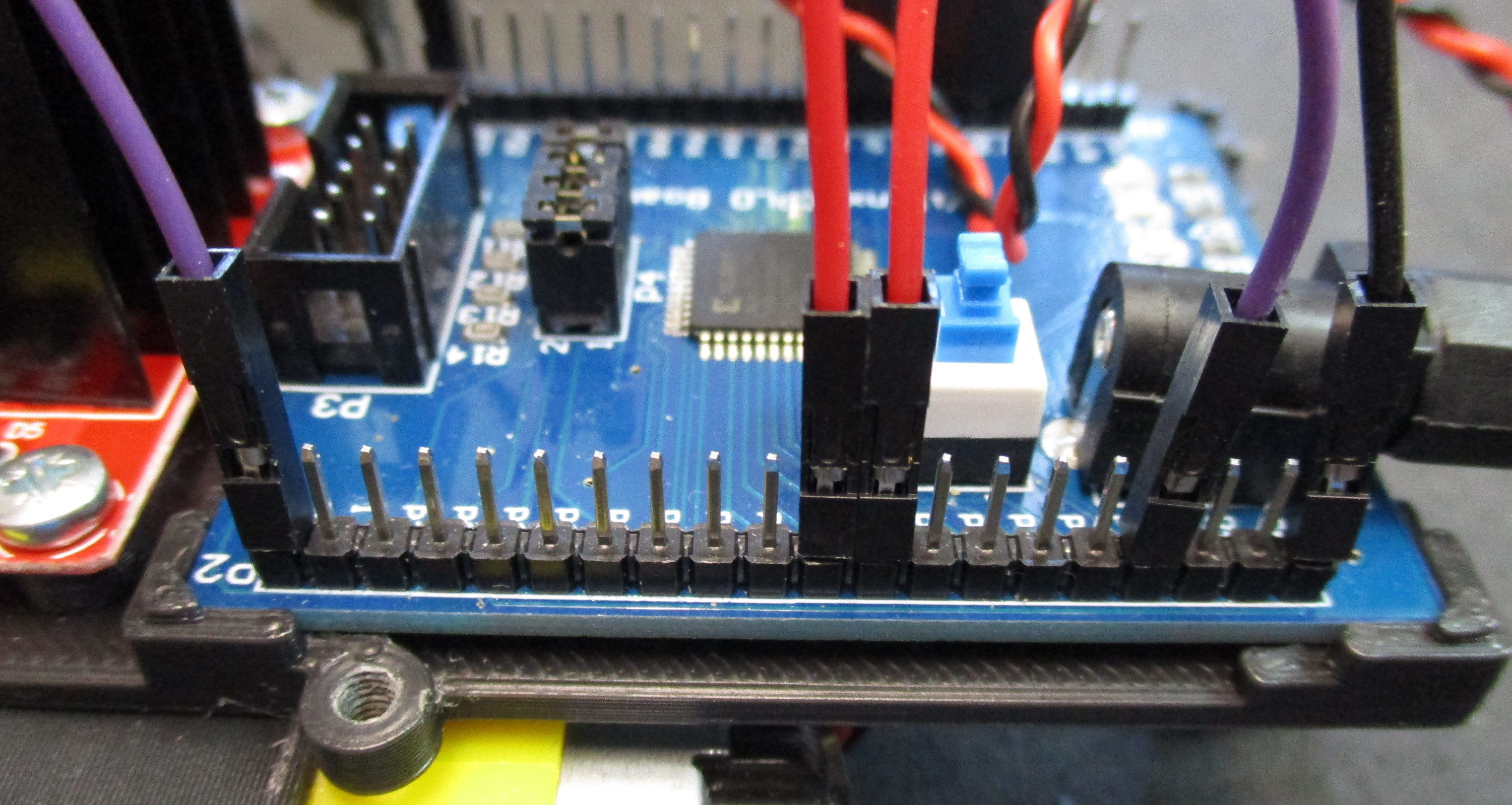
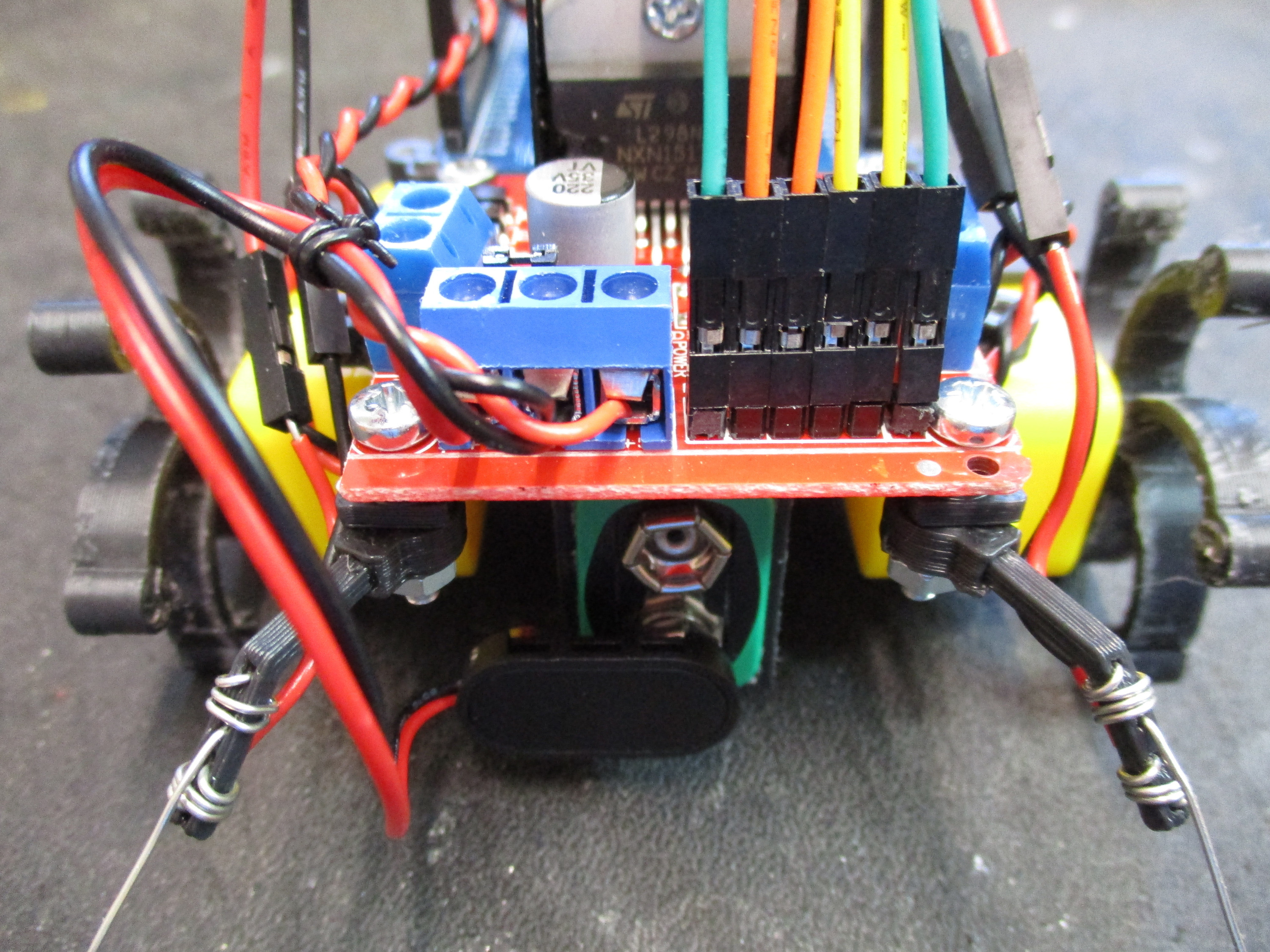
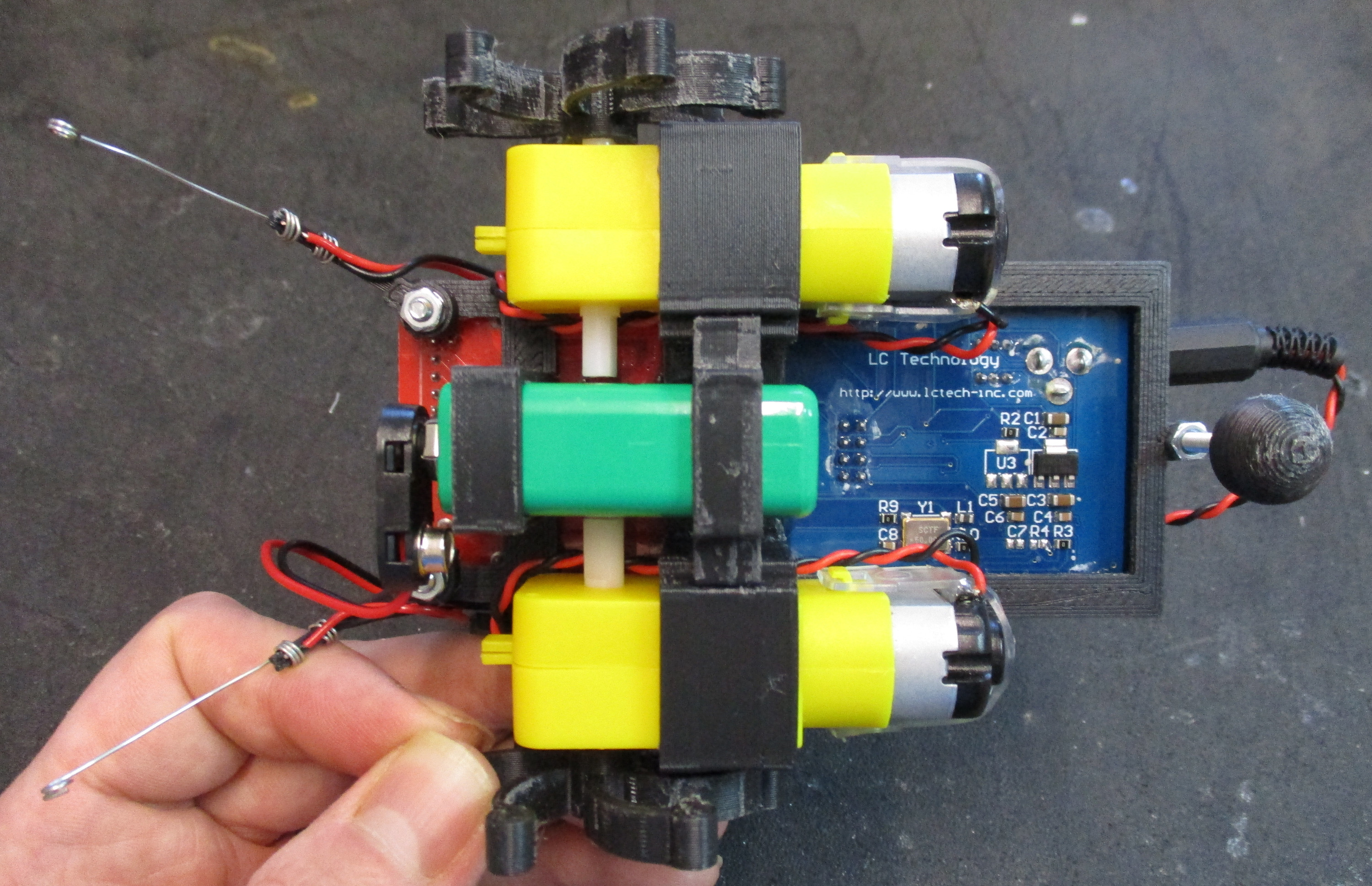
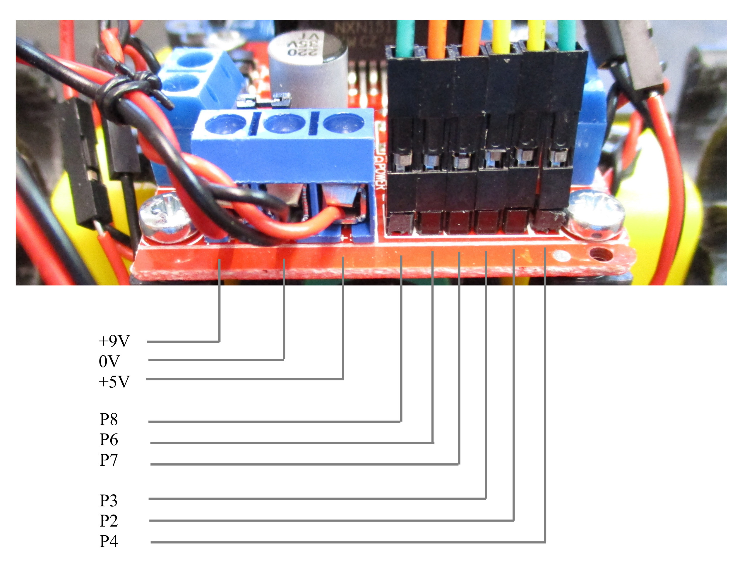
Figure 68 : wiring control signals
The first test before powering up any electronics is to give it a quick visual inspection to make sure you haven't done anything stupid e.g. i can't count the number of times ive plugged power cables in backwards, always check, check and check again. If all looks ok connect the PP3 battery, the LEDs on the motor controller and CPLD boards should turn on. If not disconnect immediately and check the battery and wiring. Note, you may need to press the CPLD power switch :)
If both LEDs turn on you can now use these Xilinx ISE projects to test the hardware. The following ISE projects use the onboard 50MHz oscillator to test out the robots basic functionality:
Test 0 : unzip test0.zip and open the ISE project, double click on Manage Configuration (Impact) to generate the .jed file and open the programming software, as shown in figure 69. Connect the robot to the USB programming cable, turn on the robot's power, you should see the programming cables status LEDs turn blue. If one LED is red this normally means that the robot is not powered / connected correctly. In the impact window double click on the Boundary scan option, then right click in the new boundary scan tab selecting initialise chain. The CPLD icon should appear, right click on this selecting program, confirm default configuration and click OK. If all has gone well a blue programming complete message should be displayed. Note, to start you robot move the reset lead from pin 27 to the 3.3V pin.
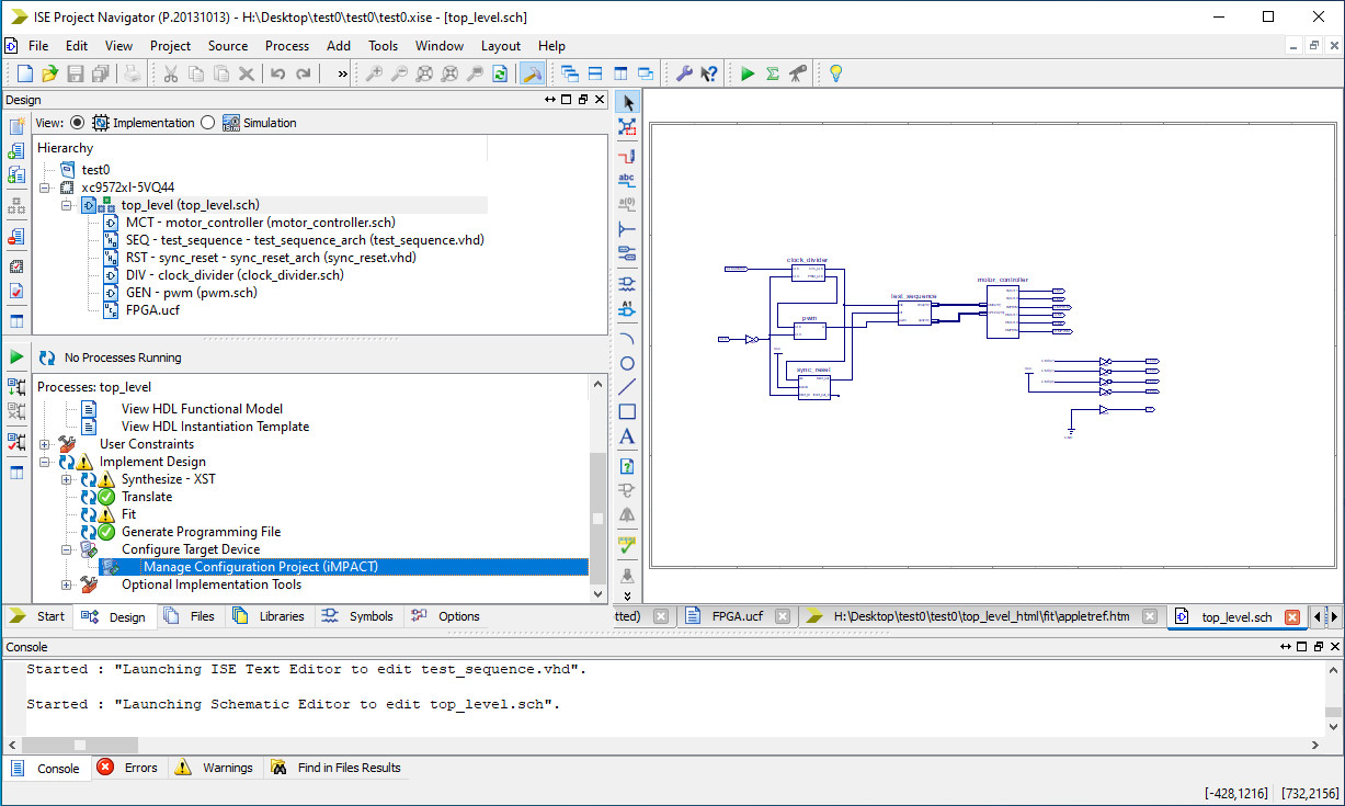
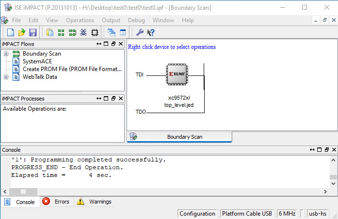
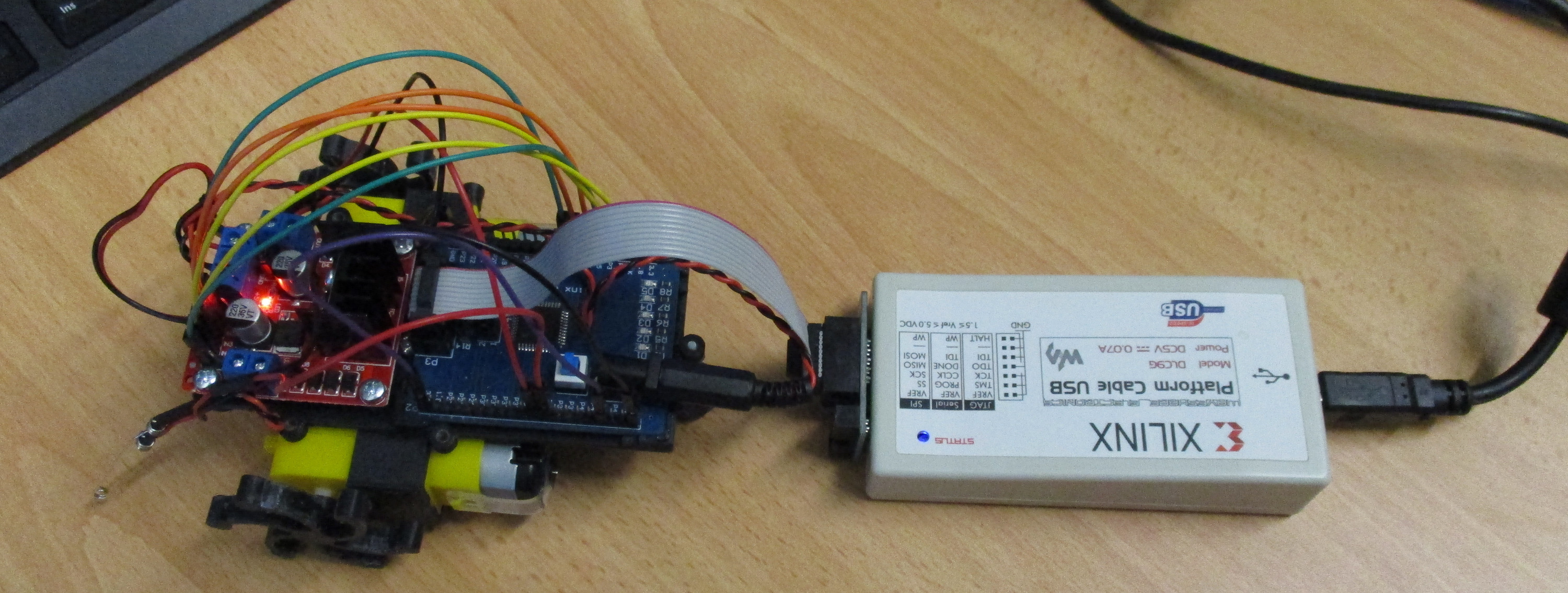

Figure 69 : configuring CPLD
This simple state machine generates a sequence of movement commands below. A short video of the robot in action is available here:(Link)
If the wheels do not rotate, check that both boards are getting power, using a multimeter check that you are getting 9V from the battery and +5V from the regulator, these can be measured from the front three-pin terminal block. If power is good, but no movement check wiring. Note, disconnect battery when you are doing this. If the wheels are not rotating in the correct directions i.e. the robot performs different movements to the video, then one or both motors have been wired in backwards. This can be corrected by swapping over the leads in the motor terminal blocks.
Test 0a : simple state machine generates a sequence of movement commands to drive a square. A short video of the robot in action is available here:(Link)
The intention of this test code is to calibrate the open loop control such that the robot performs a perfect square, well that was the intention, however, you soon find out that you get a lot of wheel spin with legged wheels and overshoot, so you will never get that perfect square without some adjustments to the control algorithms / hardware used :). However, you can make small adjustments to the PWM and system clock i.e. adding stages to the ring counter to slow down the PWM, slowing down the system clock.
Test 1 : explore and avoid obstacle behaviours as previously designed. A short video of the robot in action is available here:(Link). Discovered a small problem whilst testing these :(, within the ISE project you should be able to define internal pull-up resistors for inputs i.e. set input to default to a logic 1. These were going to be used for the pull-up resistors used in the bumper switches shown in figure 39. However, can't get these to work, therefore, had to go for additional external 4K7 resistors as shown in figure 70. These can simply be pushed into the tops of the connectors, not ideal, but it works :).
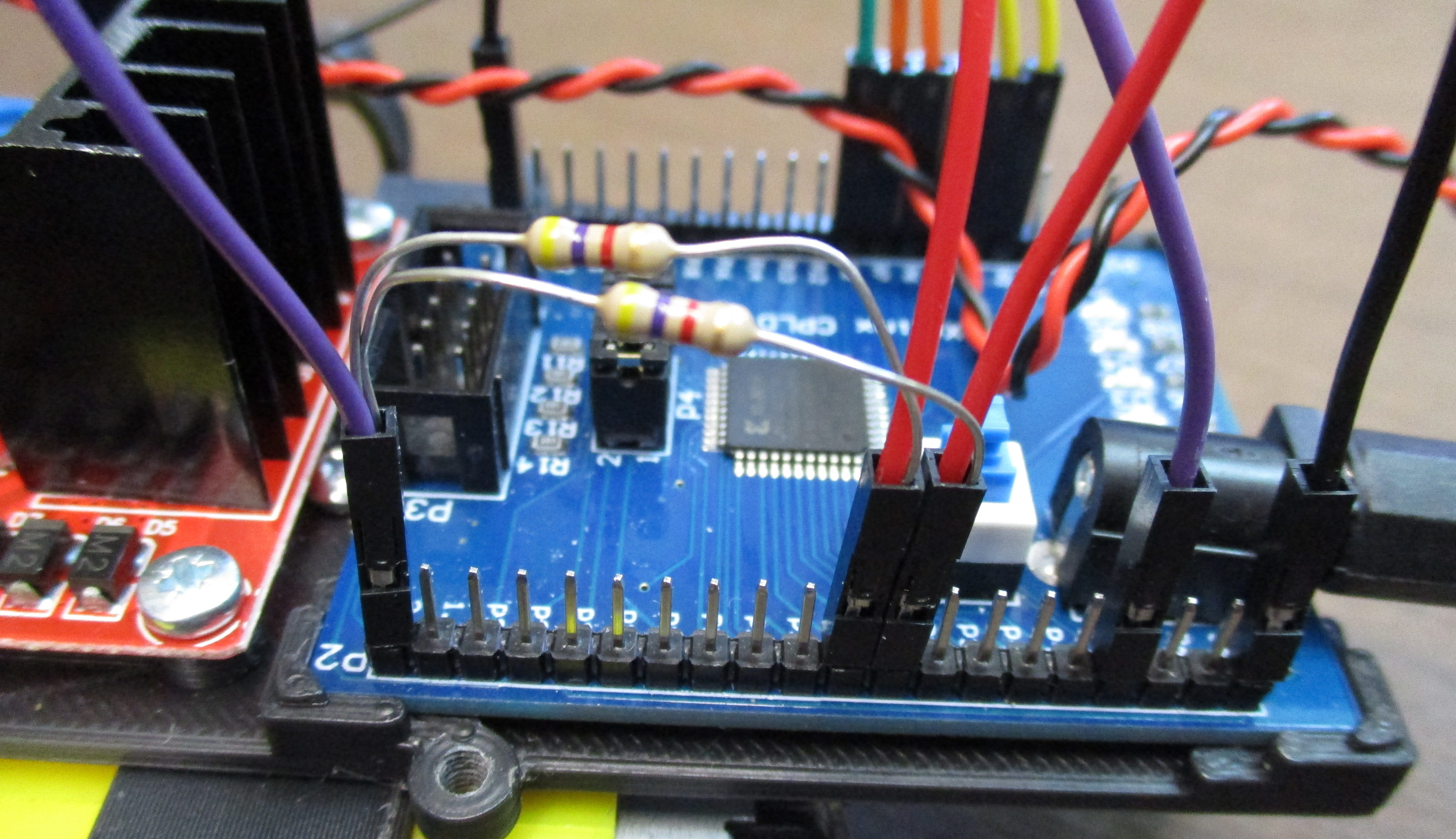
Figure 70 : external pullup resistors
Things to fix : when performing test1 i discovered a couple of bugs:
WORK IN PROGRESS

This work is licensed under a Creative Commons Attribution-NonCommercial-NoDerivatives 4.0 International License.
Contact email: mike@simplecpudesign.com