

Figure 1 : processing Bob the Bug
The original aim of the SimpleCPU architecture was to take a processor back to its fundamental basics. The goal was not to produce an optimised machine, but one that allowed students to see how a block diagram could be converted into AND gates, OR gates and Flip-flops etc. I also wanted to clearly break down the instruction phases and internal operations performed during a typical fetch-decode-execute cycle. This initial approach allows a lot of room for optimisation and improvements to increase processing performance. Therefore, as the module in which this processor was used developed i decided to update the processor i.e. make it a little more application specific, target it at some simple image processing case studies.
Program Counter - simpleCPU_v1a
Register File - simpleCPU_v1b
Register Addressing Mode - simpleCPU_v1c
Subroutines - simpleCPU_v1d
NOTE, some of the circuit diagrams are quite large, therefore, you may not be able to see signal / component names if viewed from this page. However, if you click on an image you will get a high resolution image, but some are quite large, so may take a while to load. PDFs are also available for some images.
The first improvement to consider is the Program Counter (PC). In the original design the PC is updated during a separate instruction phase, after an instruction has been executed. The reason for this implementation was to highlight this step within the CPU and reduce hardware, both in terms of routing (buses and signals) and logic gates. Taking this approach allowed the PC to be incremented using the processor's Arithmetic and Logic Unit (ALU), thus, removing the need for an additional adder i.e. converting the program "counter" into a program "register". Adding this additional adder allows the program counter to operate in parallel with the ALU i.e. performing two additions in the same clock cycle. Note, overlapping operations is commonly used in processor design to maximise performance, the downside of this parallelism is increased hardware costs i.e. to perform two additions in the same clock cycle you normally need two adders. The exception to this rule is if you double pump (clock) a functional unit i.e. run a hardware unit at double the clock speed, when compared to other hardware blocks around it. However, using different clock domains (clock speeds) can make synchronisation slightly "tricky" i.e. passing data between hardware using different clock speeds. The new program counter hardware (counter_8_v1) is shown in figure 2.
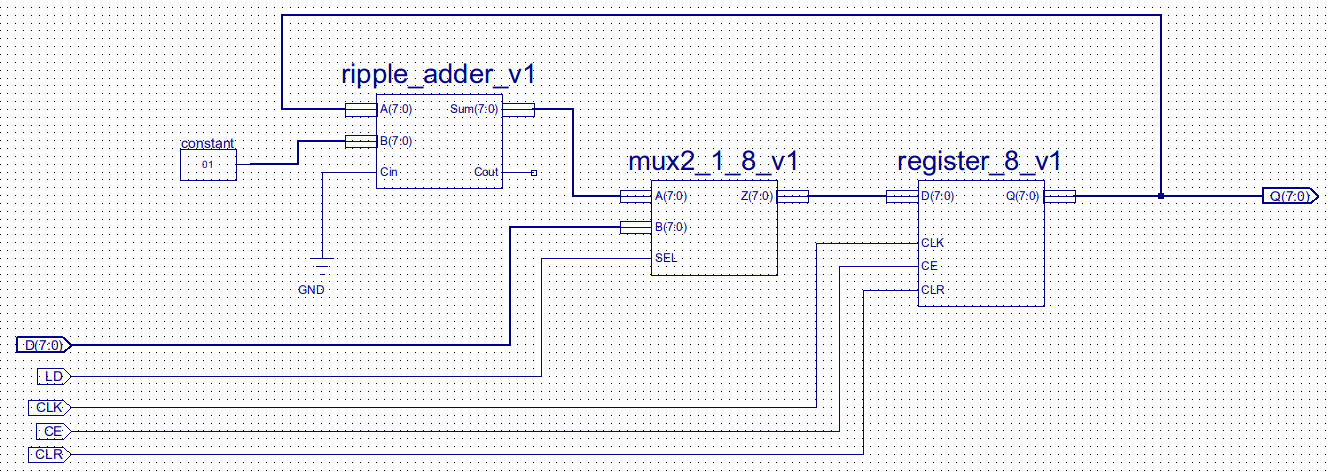
Figure 2 : new program counter
This counter reuses existing hardware components: ripple_adder_v1, mux2_1_8_v1 and register_8_v1, to implement a loadable 8bit counter. Control logic is now moved out of the decoder, adding an additional input to this component: load (LD). This is driven by the decode logic that evaluates if a conditional or unconditional jump is taken, as shown in figure 3. Note, connecting one of the inputs of the ripple adder to the constant "00000001" should cause the synthesis tools to minimise the required hardware down to an incrementer type circuit, rather than the larger general purpose adder. Performing the addition in the program counter's hardware removes the requirements for a multiplexer on input A of the ALU, therefore, also removing two 8bit buses used to pass the PC to the ALU and the incremented result back to the PC. As a result hardware increases owing to the addition of an extra adder are offset by the removal of these items. The sequence generator shown in figure 26 on the previous web page (Link) is also reduced to three flip-flops as we now only need to generate control signals for the fetch, decode and execute phases. The PC increment is now performed in parallel with the decode phase, this value being overwritten in the execute phase if a jump is taken i.e. the input to the PC (loadable counter) is now taken from the low byte of the instruction register rather than the ALU. Note, PC increment could of also been performed in parallel with the fetch. The new processor architecture (simpleCPU_v1a) is shown in figure 4.
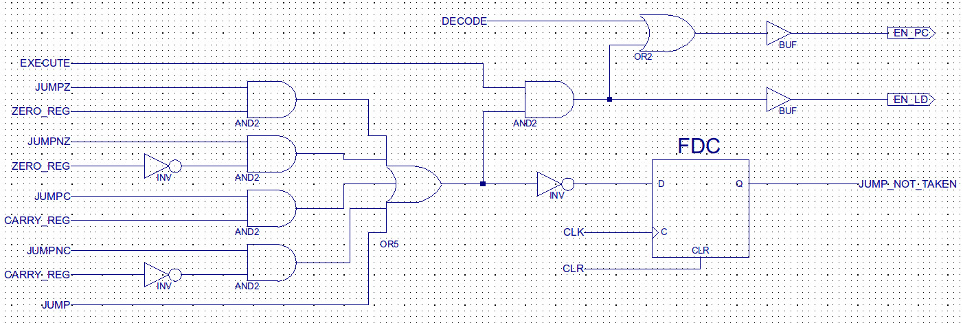
Figure 3 : program counter control logic
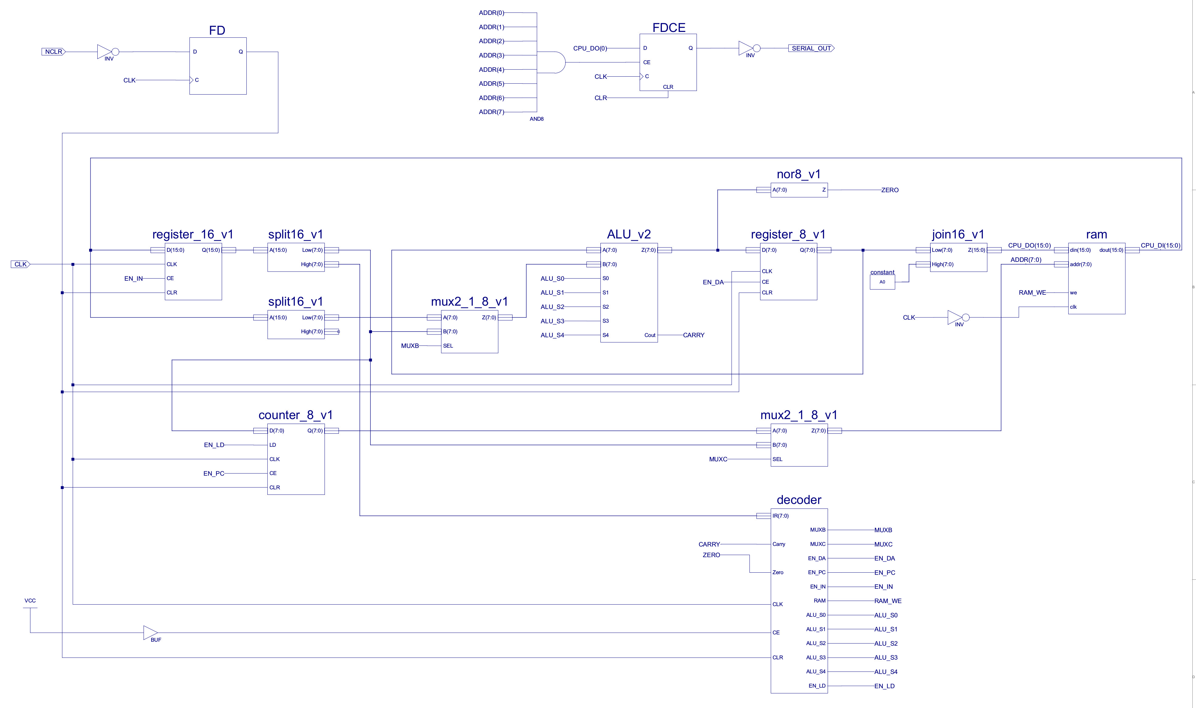
Figure 4 : simpleCPU_v1a
The new and improved SimpleCPU_v1a project files can be downloaded here: (Link). The place and routed synthesis results for the original CPU (simple_cpu_v1) and the modified version (simple_cpu_v1a) are shown below :
SIMPLE_CPU_V1
-------------
Logic Utilization:
  Number of Slice Flip Flops:            39 out of   7,168    1%
  Number of 4 input LUTs:               124 out of   7,168    1%
Logic Distribution:
  Number of occupied Slices:             82 out of   3,584    2%
  Number of bonded IOBs:                  3 out of     141    2%
  Number of RAMB16s:                      1 out of      16    6%
  Number of BUFGMUXs:                     1 out of       8   12%

SIMPLE_CPU_V1a
--------------
Logic Utilization:
  Number of Slice Flip Flops:            37 out of   7,168    1%
  Number of 4 input LUTs:               122 out of   7,168    1%
Logic Distribution:
  Number of occupied Slices:             75 out of   3,584    2%
  Number of bonded IOBs:                  3 out of     141    2%
  Number of RAMB16s:                      1 out of      16    6%
  Number of BUFGMUXs:                     1 out of       8   12%
Surprisingly overall the new version of the processor actually uses less building blocks (slices) within the FPGA. I'm guessing that this is due to the removal of the buses, multiplexer and associated simplifications of decoder logic, and the move to an additional adder that the FPGA is optimised to implement (more efficient mapping). The Xilinx tools do aggressively prune "unused" hardware to minimise FPGA usage, therefore, to double check this result was not simply due to the "efficient" tools removing logic that was actually needed, i did rerun the previous test code, all was good :). Running the processor at 4MHz to executing the above test code takes:
SIMPLE_CPU_V1  : 22.625 us
SIMPLE_CPU_V1a : 17.125 us
SPEEDUP = 32%
This speedup is simply due to reducing the number of clock cycles per instruction (CPI) from 4 to 3. Perhaps a less obvious limitation of the original architecture is that the processor only has a single general purpose register i.e. the ACC. This typically means that most algorithms will have to increase data memory accesses i.e. additional INPUT and OUTPUT instructions to access variables and intermediate results from memory. Note, this does depend on the algorithm used e.g. the performance of above test code would not be improved by the addition of more general purpose registers. However, to minimise memory traffic most modern processors do use a register file i.e. have multiple general purpose registers on-chip, reducing accesses to slower external memory. To specify within an instruction where operands are coming from and where results should be stored to, will increase the size of the instruction i.e. additional bit-fields will be required to encode which registers will be used. Fortunately the existing instruction format contains four unused bits. Therefore, this will allow a register file containing four general purpose registers e.g. RA, RB, RC and RD, to be added to the processor without having to modify the instructions or existing code.
A very simple upgrade, the ACC is replaced with a register file, to select source and destination registers a new instruction format is used as shown below:
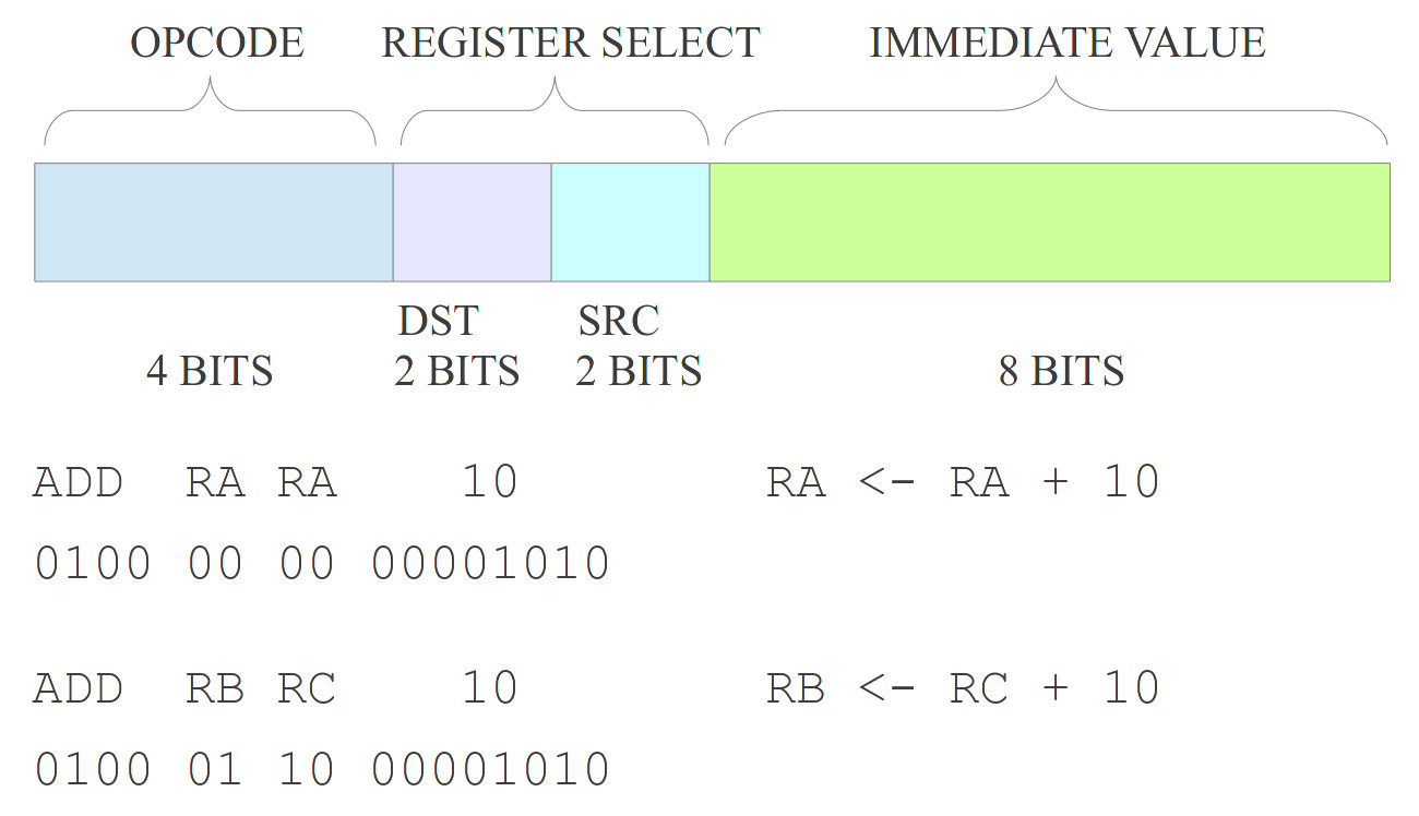
Figure 5 : new instruction format
The four bit value after the opcode is now used to encode the source and destination registers. Note, when executing the existing code RA is used as source and destination, as these bits are set to "0000". The single port register file and new top level schematic for this new processor (simpleCPU_v1b) is shown in figures 5 to 7.
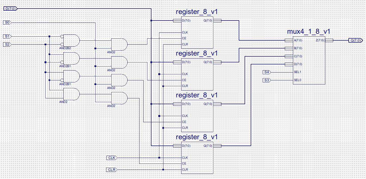
Figure 6 : single port register file
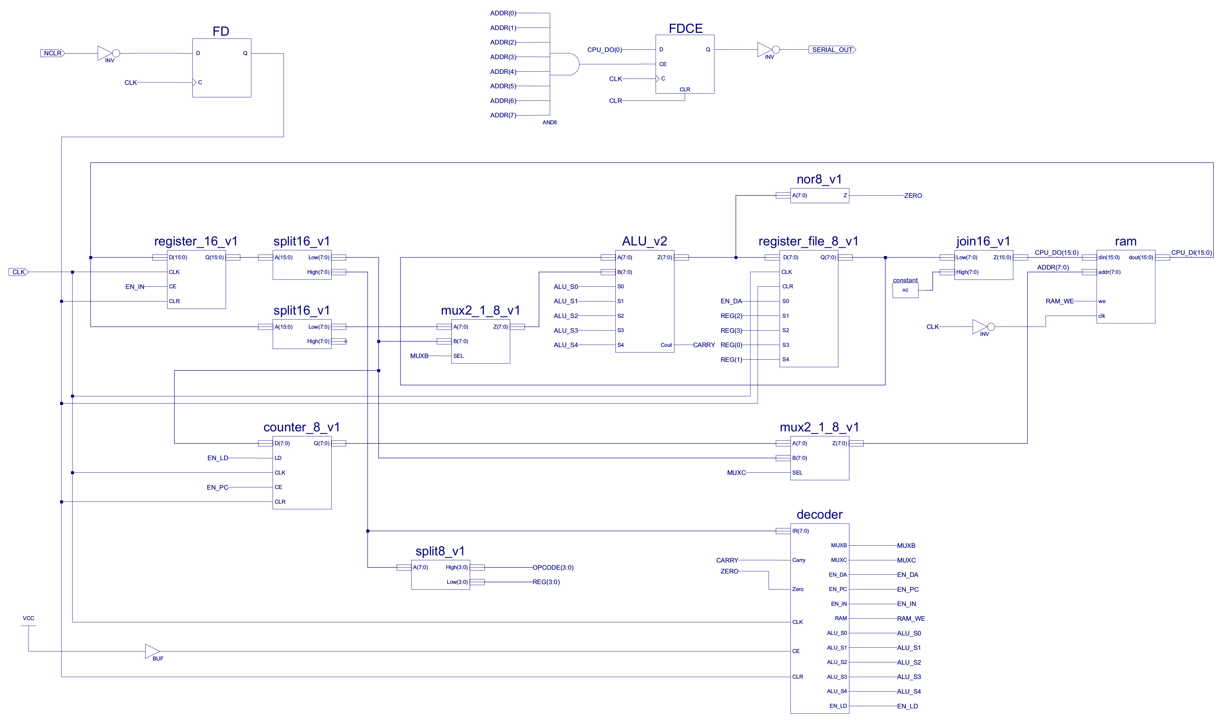
Figure 7 : simpleCPU_v1b
To test this register file the following code was used. Registers are initialised with different values, then repeatedly incremented
    DATA_RAM_WORD'("0000000000000001"), --00   LOAD RA, 0x01     - RA=1
    DATA_RAM_WORD'("0000010000000010"), --01   LOAD RB, 0x02     - RB=2
    DATA_RAM_WORD'("0000100000000011"), --02   LOAD RC, 0x03     - RC=3
    DATA_RAM_WORD'("0000110000000100"), --03   LOAD RD, 0x04     - RD=4
    DATA_RAM_WORD'("0100000000000001"), --04   ADD RA, 0x01      - INC RA
    DATA_RAM_WORD'("0100010100000001"), --05   ADD RB, 0x01      - INC RB
    DATA_RAM_WORD'("0100101000000001"), --06   ADD RC, 0x01      - INC RC
    DATA_RAM_WORD'("0100111100000001"), --07   ADD RD, 0x01      - INC RD
    DATA_RAM_WORD'("1000000000000100"), --08   JUMP 0x04         - loop
The hardware seems to work fine, waveform trace of the above test code is shown in figure 8. This processor now has four internal general purpose register, source and destination registers can be selected independently e.g. you can add the constant 32 to register RA and save the result to resister RB:
DATA_RAM_WORD'("0100010000100000"), -- ADD RB, RA, 0x20 -- RB <= RA + 32
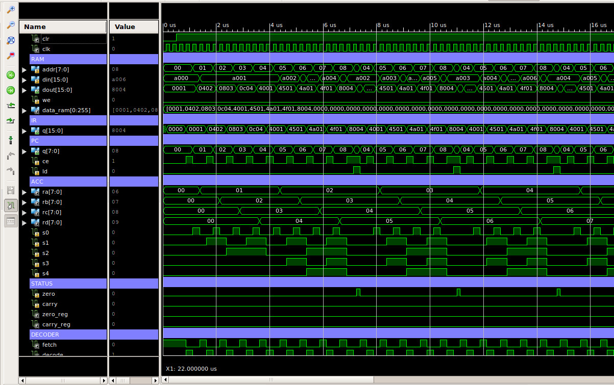
Figure 8 : test code waveform trace
The new and improved SimpleCPU_v1b project files can be downloaded here: (Link). The place and routed synthesis results for this processor are shown below :
SIMPLE_CPU_V1b
--------------
Logic Utilization:
  Number of Slice Flip Flops:            63 out of   7,168    1%
  Number of 4 input LUTs:               149 out of   7,168    2%
Logic Distribution:
  Number of occupied Slices:            102 out of   3,584    2%
  Total Number of 4 input LUTs:         149 out of   7,168    2%
  Number of bonded IOBs:                  3 out of     141    2%
  Number of RAMB16s:                      1 out of      16    6%
  Number of BUFGMUXs:                     1 out of       8   12%
As expected hardware usage has increased owing to the three extra 8bit registers, the associated multiplexer and decode logic.
In addition to allowing multiple intermediate results to be stored on the CPU, a register file also allows a new addressing mode: register addressing. Here both operands are sourced from registers and the result written back to a register. A new opcode is needed to indicate that an instruction is using register addressing, rather than immediate addressing e.g. for the ADD instruction opcodes: immediate (0100), register (1100). Also the number of read ports on the register file needs to be doubled to two, so that both operands can be read at the same time, the number of write ports does not need to be increased as this processor only has a single ALU i.e. does not produce multiple results during the execution phase, a single issue machine for the moment :). When using the register addressing mode, the lower eight bits of the instruction are now no longer required to represent an immediate value, therefore, using these spare "bits" there are a couple of different ways of encoding this addressing mode, as shown below:
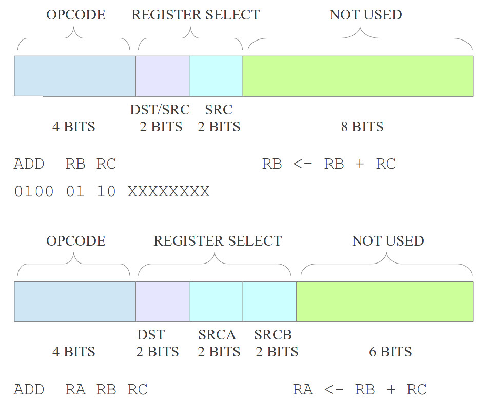
Figure 9 : new instruction format
The advantage of the first format is that the instruction is more compact, can reuse the same decode hardware within the register file. The advantage of the second format is that it allows full flexibility, allowing any combination of source and destination registers. This can be useful when implementing an algorithm, as the first format will overwrite one of the operands with the result i.e. if this data is then needed in a later calculation this value will need to be stored in data memory, incurring the associated INPUT / OUTPUT instructions needed to re-load this variable back into the CPU, so that it can be processed (remember ALU can not process data in memory directly, it must be in registers). The disadvantage of the second format is that the register file will need additional decode logic to select this second operand register. Whatever format is used the multiplexer on the B input of the ALU will need to be modified (note will come back to this decision later), an additional input will need to be added to access the second read port from the register file, as shown in figures 9 to 11.
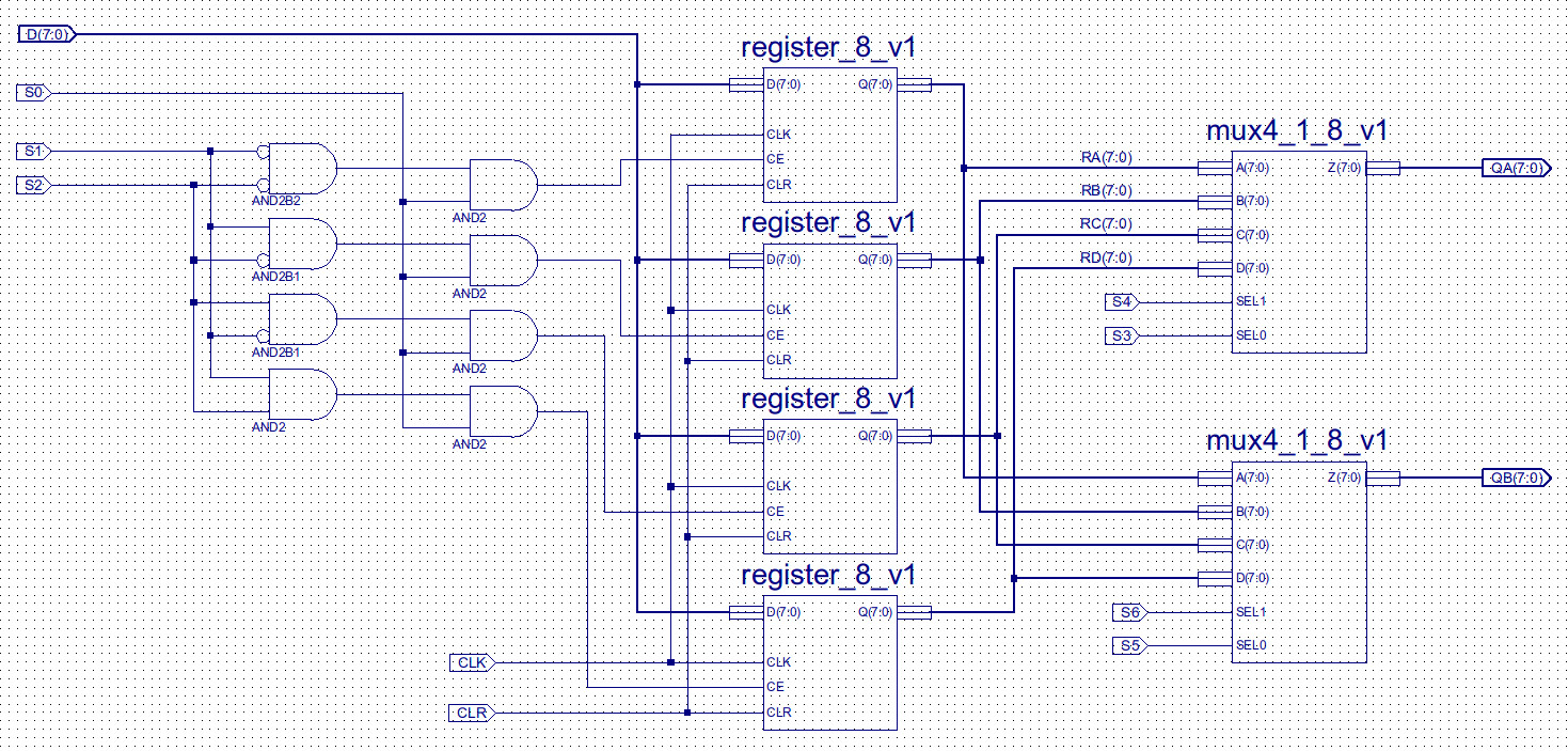
Figure 10 : dual port register file, single write port (D), dual read port (QA) and (QB)
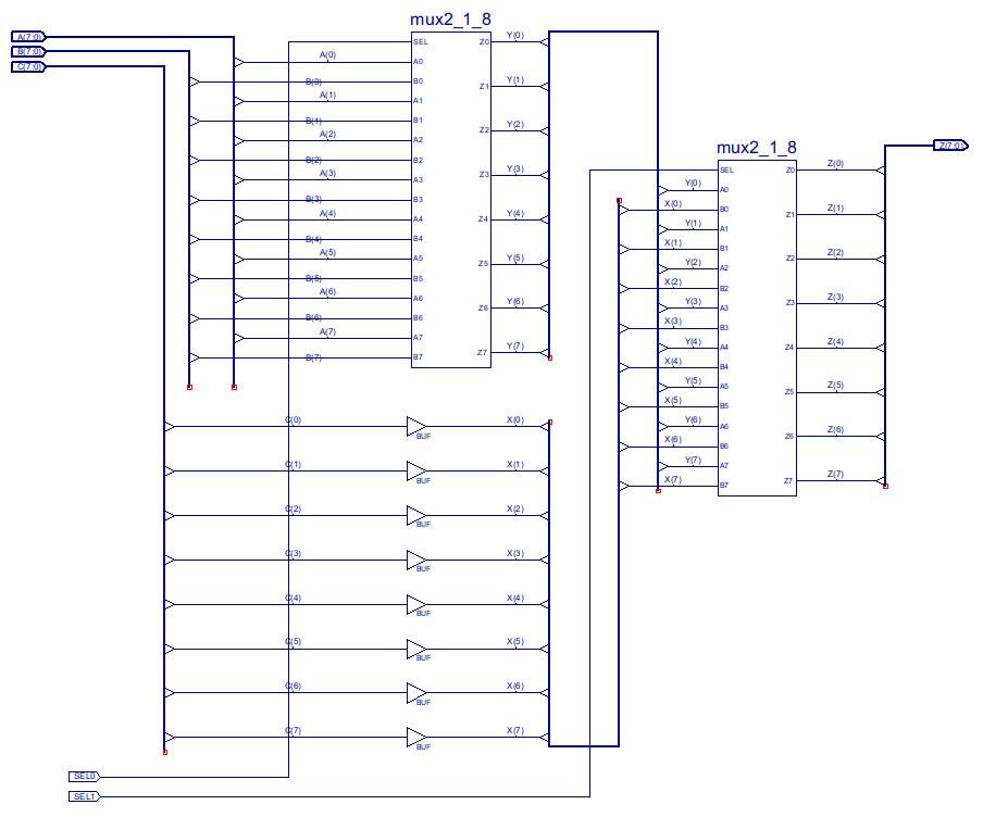
Figure 11 : three input MUX - note longer signal path for A and B, compared to C
Now the fun bit :(, adding a new instruction into a hardwired controller is a pain, you need to update the decode logic for all the associated control signals and functional blocks, as shown in figures 12 and 13 (ADD_R control signal). Do confess this is not an optimal solution, but i did not have time (couldn't be bothered) to do a "proper" minimisation, especially as the Xilinx tools will "do" this automatically for you. Note, in a real design never trust automatic synthesis tools, sometimes they can produce strange results, its always a good idea to double check they have produced something that is in the ball park of what you were expecting. The approach taken to implement this hardwired controller is to first decode the opcode into a one-hot representation, then using the control-signal table shown in figure 31 on the previous web page (Link), combine these active (hot) bits to generate the required logic '1' control signals i.e. each column in the table is generated by an OR gate, the number of 1s in the column define the OR gates fan-in (number of inputs). This does not produce a fully minimised decoder, but its quick to implement.
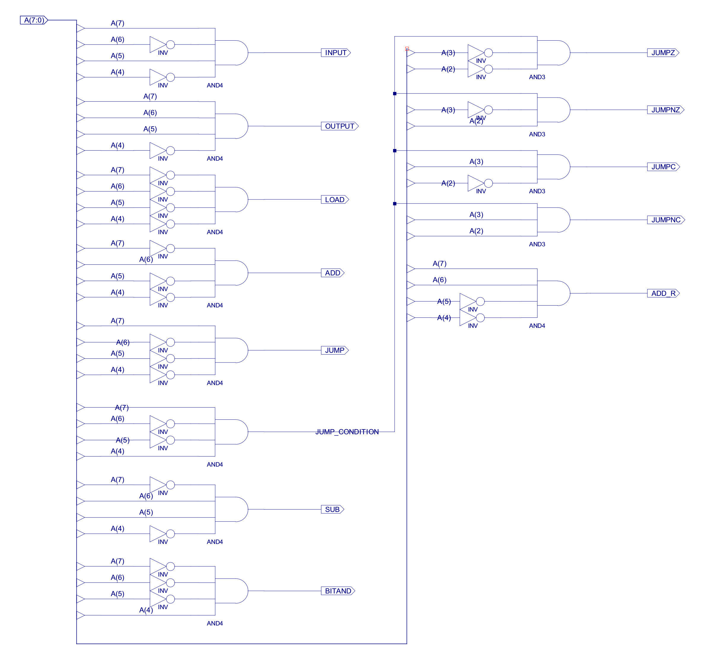
Figure 12 : Instruction decoder - addition of ADD_R (bottom right)
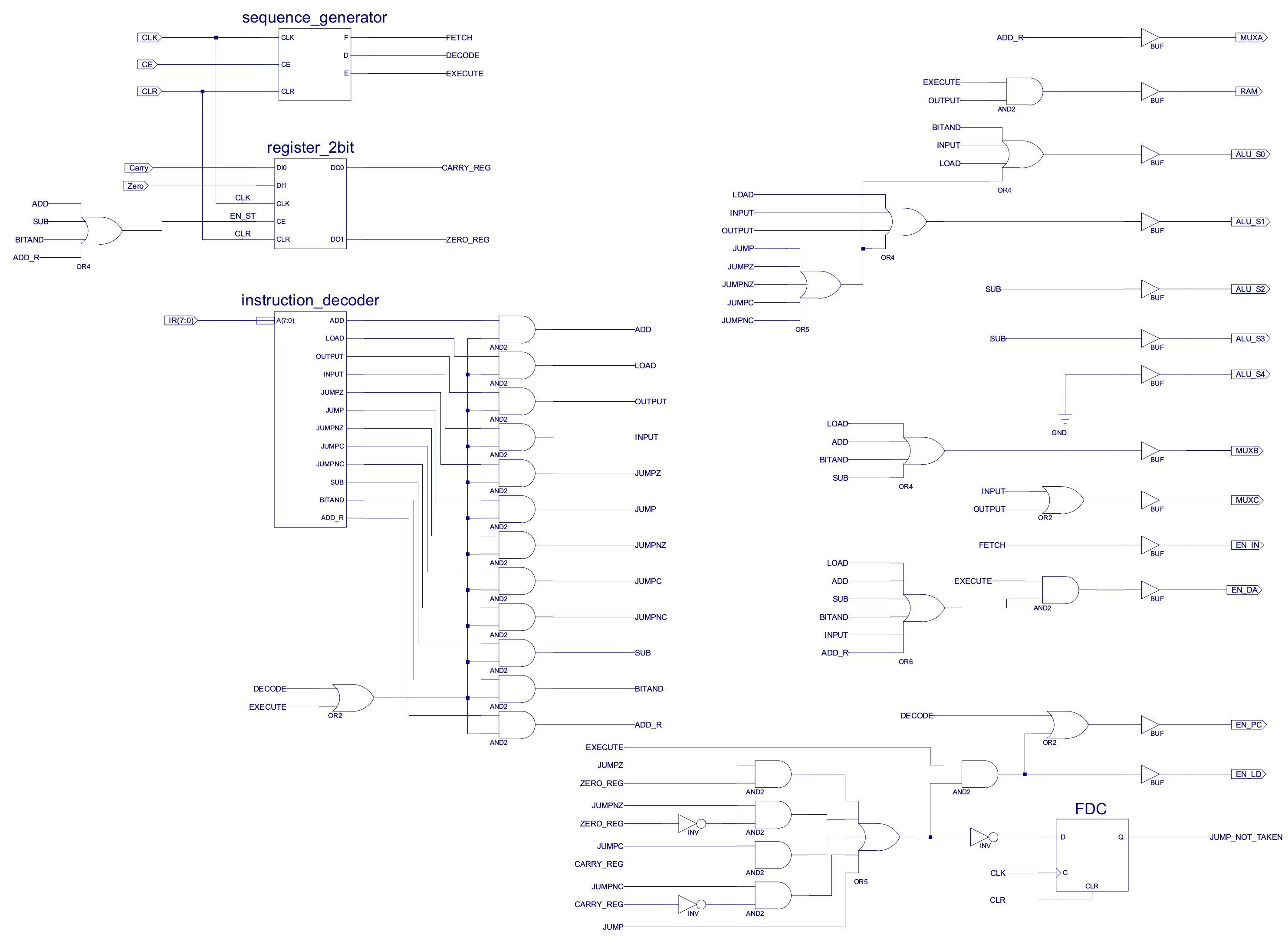
Figure 13 : Complete instruction decoder
The top level schematic of this new CPU (simpleCPU_v1c) is shown in figure 14, the project files can be downloaded here: (Link). The main difference is the extra read port on the register file and associated bus and multiplexer input.
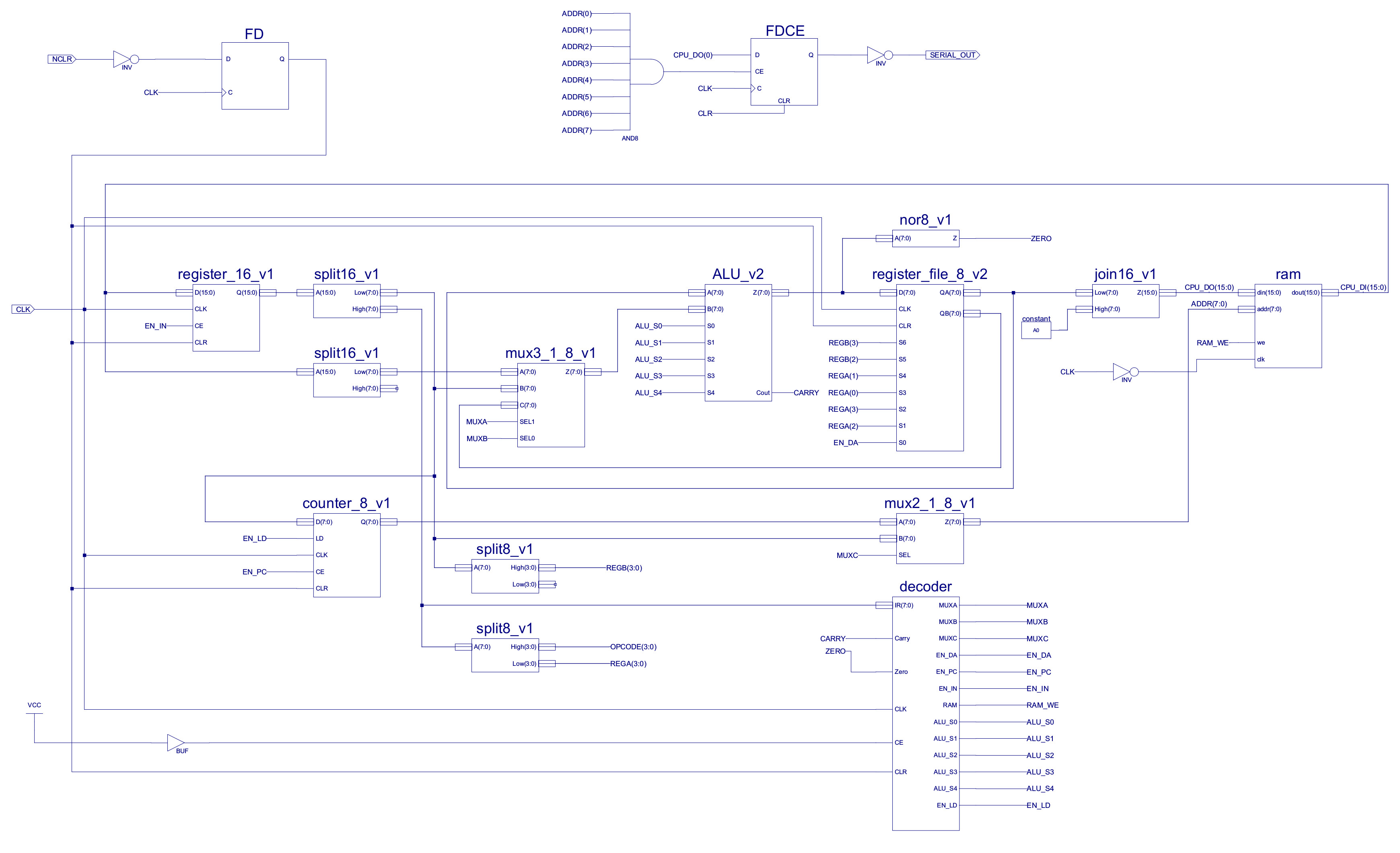
Figure 14 : simpleCPU_v1c
To test this register file the previous test code was modified, as shown below. Registers are initialised with different values, then repeatedly incremented
    DATA_RAM_WORD'("0000000000000001"), --00   LOAD RA, 0x01     - RA=1
    DATA_RAM_WORD'("0000010000000010"), --01   LOAD RB, 0x02     - RB=2
    DATA_RAM_WORD'("0000100000000011"), --02   LOAD RC, 0x03     - RC=3
    DATA_RAM_WORD'("0000110000000100"), --03   LOAD RD, 0x04     - RD=4
    DATA_RAM_WORD'("0100000000000001"), --04   ADD RA, 0x01      - INC RA     - RA=2
    DATA_RAM_WORD'("0100010100000001"), --05   ADD RB, 0x01      - INC RB     - RB=3
    DATA_RAM_WORD'("0100101000000001"), --06   ADD RC, 0x01      - INC RC     - RC=4
    DATA_RAM_WORD'("0100111100000001"), --07   ADD RD, 0x01      - INC RD     - RD=5
    DATA_RAM_WORD'("1100000000000000"), --08   ADD RA, RA, RA    - RA = RA+RA - RA=4
    DATA_RAM_WORD'("1100000110000000"), --09   ADD RA, RB, RC    - RA = RB+RC - RA=3+4=7
    DATA_RAM_WORD'("1100001011000000"), --0A   ADD RA, RC, RD    - RA = RC+RD - RA=4+5=9
    DATA_RAM_WORD'("1100100100000000"), --0B   ADD RC, RB, RA    - RC = RB+RA - RC=3+9=12
    DATA_RAM_WORD'("1000000000000100"), --0C   JUMP 0x04         - loop
Again all seemed to work ok, waveform trace of register updates shown in figure 15, showing the values of RA,RB,RC and RD as each instruction is executed.
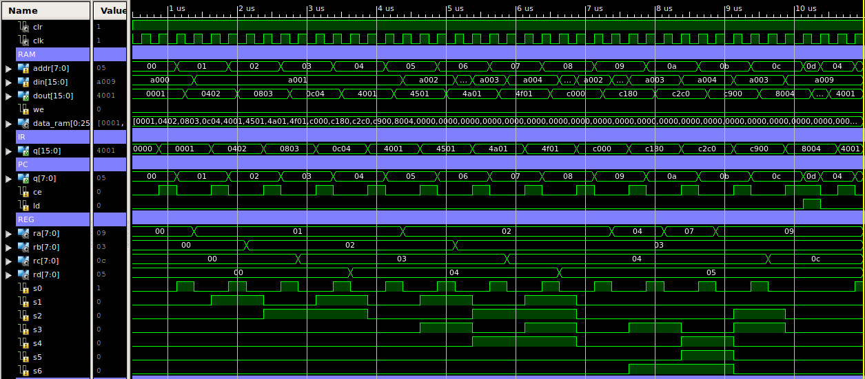
Figure 15 : test code waveform trace
As hinted previously, expanding the ALU's multiplexer from two inputs to three inputs may have not been the best choice. The advantage of this solution was that some of the existing logic in the instruction decoder could be reused e.g. output MUXB. The disadvantage is that it increases the critical path delay (CPD), as there are now two two-input multiplexers in series, as shown in figure 14. This may reduce the processor's maximum clock speed, as signals will now take longer to travel through this logic, reducing performance as less instructions will be executed per second :(. The reason why increases in the CPD reduces the CPU's clock speed is shown in figure 16. You can consider the processors hardware as a collection of flip-flops linked together by logic. The first flip-flop in figure 16 is the signal source e.g. the instruction register (IR), the second is the destination e.g. the register file (RA,RB,RC or RD). The clock period must be select such that the output of the logic e.g. ALU, has sufficient time to settle to a stable final value, this delay is determined by the propagation delay of the logic gate and routing / wire delays. If you were to try and clock the processor faster than this delay, invalid data (intermediate results) would be store in the output flip-flop.
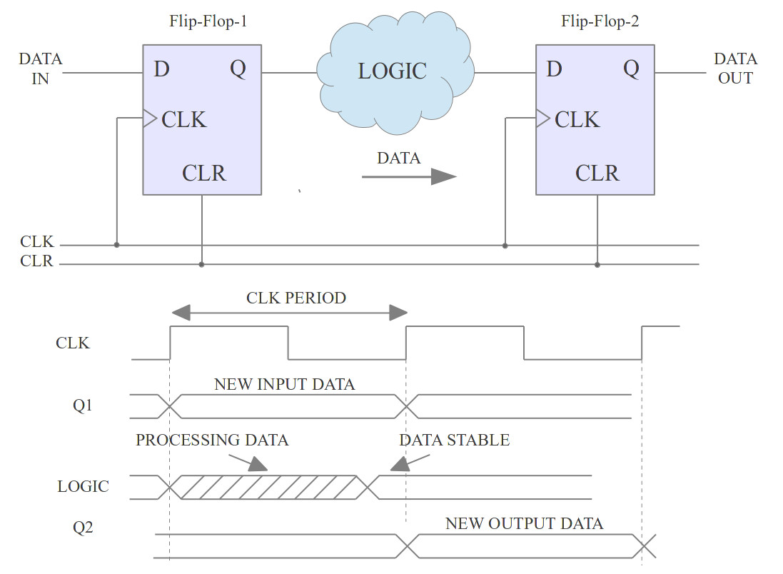
Figure 16 : hardware - critical path delay
When designing a processor this is always a key consideration, ideally we would like to minimise signal delays, however, this is not always possible i.e. we need logic gates to implement the desired functions. Also sometimes some of the worst signal delays are simply due to the time it takes for a signal to travel from one side of the FPGA to the other i.e. wire delays. Identifying the CPD can be estimated by simply looking at the block diagram, however, fortunately the Xilinx tools will identify this for you. For this processor the CPD is:
Delay:               43.607ns (Levels of Logic = 36)
  Source:            IR/XLXI_2/XLXI_21/XLXI_1 (FF)
  Destination:       INSTR_DECODER/XLXI_4/XLXI_2 (FF)
  Source Clock:      CLK rising
  Destination Clock: CLK rising

  Data Path: IR/XLXI_2/XLXI_21/XLXI_1 to INSTR_DECODER/XLXI_4/XLXI_2
                                Gate     Net
    Cell:in->out      fanout   Delay   Delay  Logical Name (Net Name)
    ----------------------------------------  ------------
     FDCE:C->Q             1   0.626   0.681  IR/XLXI_2/XLXI_21/XLXI_1 (INSTR<12>)
     BUF:I->O             10   0.479   0.964  IR_SPLIT/XLXI_4 (IR_HIGH<4>)
     INV:I->O              1   0.479   0.681  INSTR_DECODER/XLXI_55/XLXI_108 (INSTR_DECODER/XLXI_55/XLXN_181)
     AND4:I0->O            1   0.479   0.681  INSTR_DECODER/XLXI_55/XLXI_110 (INSTR_DECODER/XLXN_773)
     AND2:I1->O            5   0.479   0.783  INSTR_DECODER/XLXI_321 (INSTR_DECODER/SUB)
     OR4:I0->O             1   0.479   0.681  INSTR_DECODER/XLXI_360 (INSTR_DECODER/XLXN_226)
     BUF:I->O             16   0.479   1.051  INSTR_DECODER/XLXI_11 (MUXB)
     INV:I->O              1   0.479   0.681  ALU_MUX/XLXI_1/XLXI_1/XLXI_4 (ALU_MUX/XLXI_1/XLXI_1/XLXN_2)
     AND2:I0->O            1   0.479   0.681  ALU_MUX/XLXI_1/XLXI_1/XLXI_1 (ALU_MUX/XLXI_1/XLXI_1/XLXN_5)
     OR2:I1->O             1   0.479   0.681  ALU_MUX/XLXI_1/XLXI_1/XLXI_3 (ALU_MUX/Y<0>)
     AND2:I1->O            1   0.479   0.681  ALU_MUX/XLXI_3/XLXI_1/XLXI_1 (ALU_MUX/XLXI_3/XLXI_1/XLXN_5)
     OR2:I1->O             3   0.479   0.771  ALU_MUX/XLXI_3/XLXI_1/XLXI_3 (MUX_B_DATA<0>)
     XOR2:I1->O            1   0.479   0.681  ALU/XLXI_5/XLXI_8 (ALU/XLXN_90<0>)
     AND2:I0->O            2   0.479   0.745  ALU/XLXI_19/XLXI_1 (ALU/XLXN_60<0>)
     XOR2:I0->O            2   0.479   0.745  ALU/XLXI_1/FA0/HA0/XLXI_2 (ALU/XLXI_1/FA0/XLXN_7)
     AND2:I1->O            1   0.479   0.681  ALU/XLXI_1/FA0/HA1/XLXI_1 (ALU/XLXI_1/FA0/XLXN_2)
     OR2:I0->O             2   0.479   0.745  ALU/XLXI_1/FA0/XLXI_3 (ALU/XLXI_1/XLXN_1)
     AND2:I0->O            1   0.479   0.681  ALU/XLXI_1/FA1/HA1/XLXI_1 (ALU/XLXI_1/FA1/XLXN_2)
     OR2:I0->O             2   0.479   0.745  ALU/XLXI_1/FA1/XLXI_3 (ALU/XLXI_1/XLXN_12)
     AND2:I0->O            1   0.479   0.681  ALU/XLXI_1/FA2/HA1/XLXI_1 (ALU/XLXI_1/FA2/XLXN_2)
     OR2:I0->O             2   0.479   0.745  ALU/XLXI_1/FA2/XLXI_3 (ALU/XLXI_1/XLXN_27)
     AND2:I0->O            1   0.479   0.681  ALU/XLXI_1/FA3/HA1/XLXI_1 (ALU/XLXI_1/FA3/XLXN_2)
     OR2:I0->O             2   0.479   0.745  ALU/XLXI_1/FA3/XLXI_3 (ALU/XLXI_1/XLXN_32)
     AND2:I0->O            1   0.479   0.681  ALU/XLXI_1/FA4/HA1/XLXI_1 (ALU/XLXI_1/FA4/XLXN_2)
     OR2:I0->O             2   0.479   0.745  ALU/XLXI_1/FA4/XLXI_3 (ALU/XLXI_1/XLXN_37)
     AND2:I0->O            1   0.479   0.681  ALU/XLXI_1/FA5/HA1/XLXI_1 (ALU/XLXI_1/FA5/XLXN_2)
     OR2:I0->O             2   0.479   0.745  ALU/XLXI_1/FA5/XLXI_3 (ALU/XLXI_1/XLXN_101)
     AND2:I0->O            1   0.479   0.681  ALU/XLXI_1/FA6/HA1/XLXI_1 (ALU/XLXI_1/FA6/XLXN_2)
     OR2:I0->O             2   0.479   0.745  ALU/XLXI_1/FA6/XLXI_3 (ALU/XLXI_1/XLXN_103)
     XOR2:I0->O            1   0.479   0.681  ALU/XLXI_1/FA7/HA1/XLXI_2 (ALU/XLXN_1<7>)
     AND2:I1->O            1   0.479   0.681  ALU/XLXI_3/XLXI_1/XLXI_16/XLXI_1 (ALU/XLXI_3/XLXI_1/XLXI_16/XLXN_5)
     OR2:I1->O             1   0.479   0.681  ALU/XLXI_3/XLXI_1/XLXI_16/XLXI_3 (ALU/XLXI_3/Y<7>)
     AND2:I1->O            1   0.479   0.681  ALU/XLXI_3/XLXI_3/XLXI_16/XLXI_1 (ALU/XLXI_3/XLXI_3/XLXI_16/XLXN_5)
     OR2:I1->O             5   0.479   0.783  ALU/XLXI_3/XLXI_3/XLXI_16/XLXI_3 (ALU_DATA<7>)
     begin scope: 'ZERO_DETECT/XLXI_1'
     OR4:I0->O             1   0.479   0.681  I_36_110 (S0)
     NOR2:I0->O            1   0.479   0.681  I_36_140 (O_DUMMY)
     end scope: 'ZERO_DETECT/XLXI_1'
     FDCE:D                    0.176          INSTR_DECODER/XLXI_4/XLXI_2
    ----------------------------------------
    Total                     43.607ns (17.567ns logic, 26.040ns route)
                                       (40.3% logic, 59.7% route)
This listing can be a little hard to follow, but, basically the CPD path is:
  IR_REG -> INSTR_DECODER -> ALU_MUX -> ALU -> ZERO_DETECT -> STATUS_REG
    FF            |______________LOGIC________________|           FF
So the question is: is it worth redesigning the data paths to the ALU i.e. reverting back to using two two-input multiplexers, one multiplexer on each ALU input, switching operand data buses: memory, instruction register, register file QA, or register file QB. Maybe, but looking at the above CPD analysis, the ALU_MUX delay does not look that significant compared to all the other delays, so will leave this one for now.
As identified from the previous "Hello World" test program, sometimes you need to use the same code in different parts of the program e.g. a software delay loop. Therefore, most processors support subroutines through the use of CALL and RETURN instructions (names will vary). To implement this functionality the CPU's hardware needs to be able to make a copy of the current PC value, so that the program knows where to return back to after it has finished the subroutine (function), as shown in figure 17.
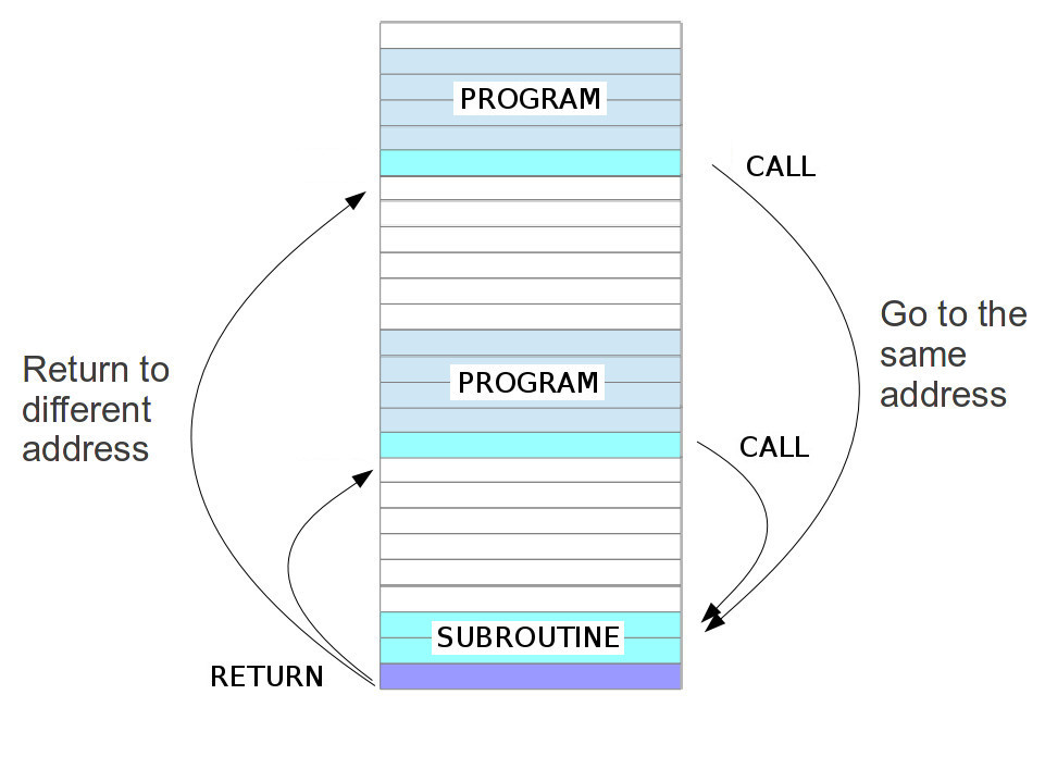
Figure 17 : subroutine CALL and RETURN
In this example the CALL instruction is comparable to a modified unconditional JUMP. Both the CALL and JUMP instructions contain the address of the instruction that should be executed next i.e. for the CALL instruction the address of the first instruction of the subroutine (function). Where they differ is that the CALL instruction also stores the current PC value to memory, such that when the RETURN instruction is executed at the end of the subroutine to program can jump back to from whence it came i.e. the next instruction after the original CALL (the processor loads the old PC+1 into the PC). In the early days of computing one of the first machines to use subroutines i.e. libraries of pre-written code was EDSAC (Link). This processor also had a very simple instruction set, very comparable to simpleCPU. To implement subroutines this machine would perform a "Wheeler jump", named after David Wheeler, one of the designers. This approach used self modifying code to rewrite the program each time a subroutine was executed e.g. the RETURN instruction was implemented using an unconditional jump, where the jump instruction's address field was over written at run-time, such that the program returned to the correct point within the main program each time the subroutine was performed. Self modifying code is a very bad idea i.e. a program that rewrites its instructions at run-time, however, it does simplify the hardware :). Also i like it from a teaching view point as it illustrates the "difference", or lack of, between an instructions and data i.e. a processor only sees patterns 1's and 0's. Therefore, for better or worse i'm going to recreate the "Wheeler Jump" in honour of EDSAC. To implement this approach the processor needs to be expanded to a 16bit machine i.e. the ALU's data buses needs to be the same width as the instruction. This is relatively "simple" to implement as it does not changes the instruction decoder, all that needs to be modified (expand) is the ALU, REGISTER_FILE, MUX and data buses to 16bits, but there are a LOT of components to update :(. This is where i decided to finish work on this version of the processor, it soon became evident that i needed a complete rework, therefore, started versions 1av1, 2 and 3...

This work is licensed under a Creative Commons Attribution-NonCommercial-NoDerivatives 4.0 International License.
Contact email: mike@simplecpudesign.com