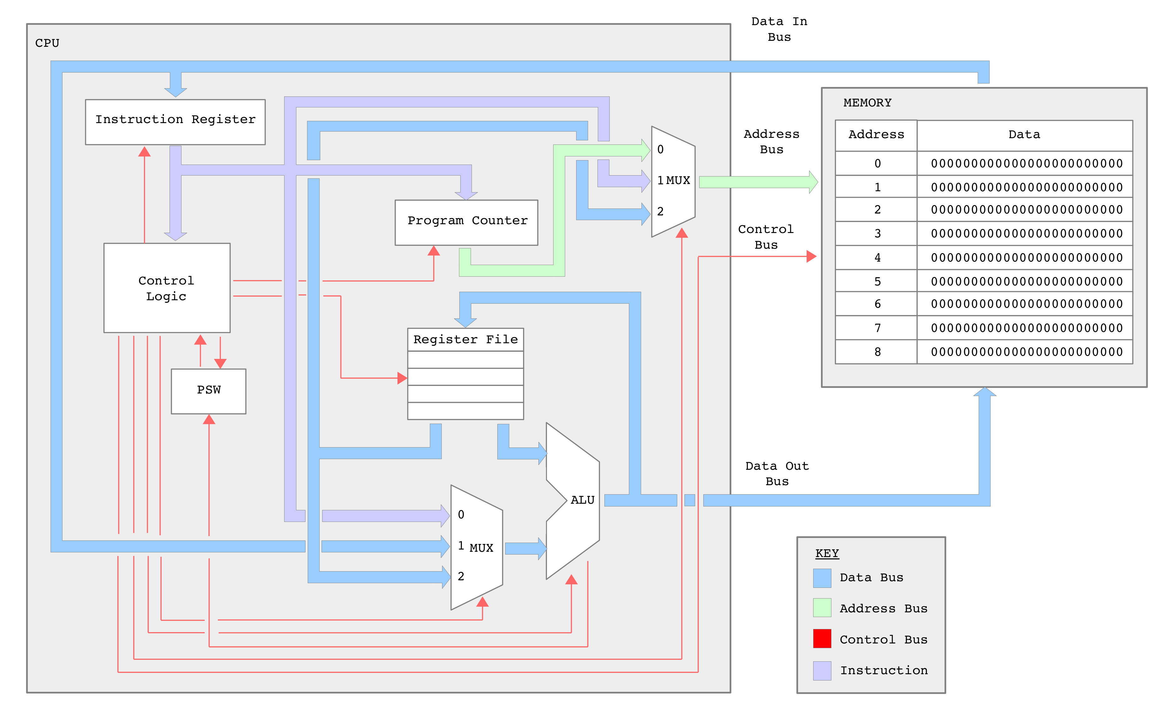
Figure 1 : simpleCPU_v1d block diagram
Another day, another dollar, another processor :). The simpleCPU_v1a has a few fundamental flaws that limits its practical usage. These limitations were by design i.e. you don't know what you have and why you need them until they are gone. This version of the processor removes some of these failings:
The new and improved ISE project files for this processor can be downloaded here: (Link), its top level schematic and block diagram are shown in figures 1 and 2. Basically the same structure, but with a few tweaks and improvements. A python based assembler is also available here: (Link).
Improvement 1 : increase external memory size
Improvement 2 : increase internal memory size and width
Improvement 3 : New addressing modes - Register, Register Indirect
Improvement 4 : Subroutines
Improvement 5 : Control logic
Improvement 6 : Data MUX
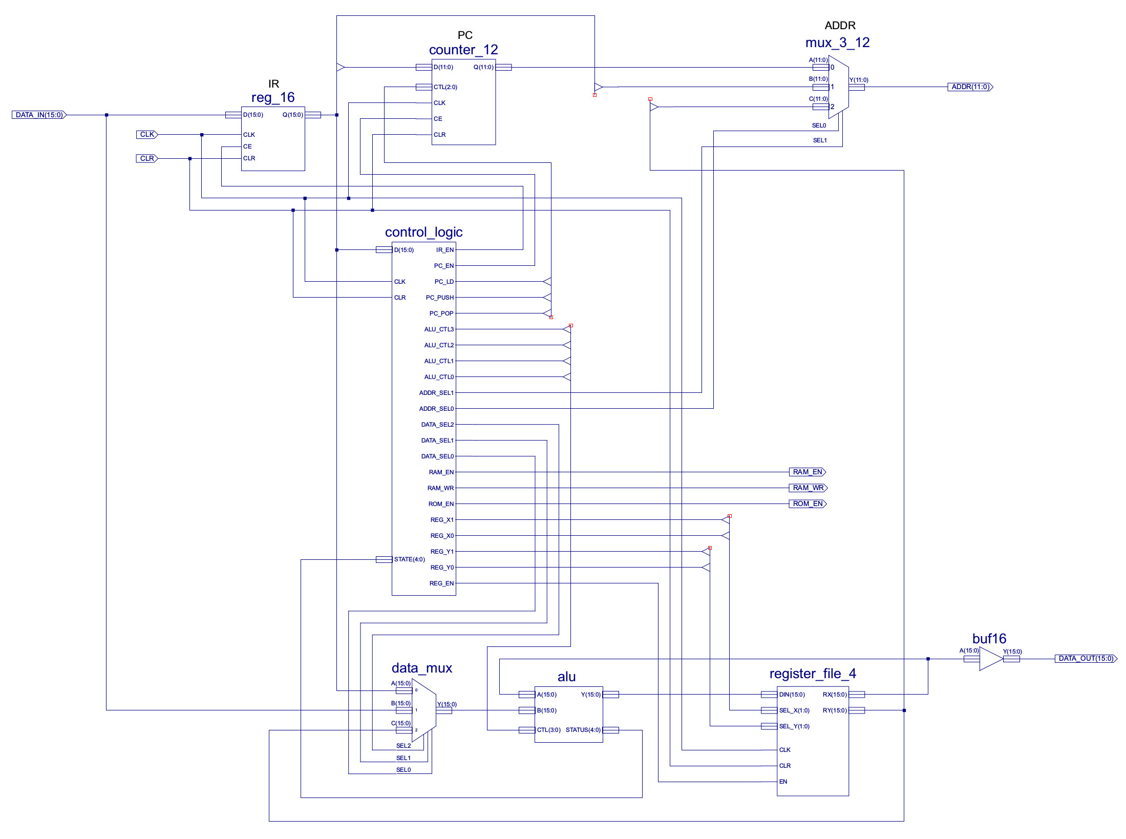
Figure 2 : simpleCPU_v1d ISE schematic
Version 1a of the processor could only address 256 x 16 bit memory locations, this doesn't leave a lot of room for a system's functions e.g. the original LCD version of HELLO WORLD needed 221 instructions. Therefore, the SimpleCPU_v1d memory size is increased to 4096 x 16 bit memory locations. When designing processors you soon realise that the hardware used is highly coupled i.e. small changes in one part of the system tend to ripple through the design into others. In the land of hardware there is no such thing as a "small change", hardware is not software :). When increasing the processor's memory size, the question arises "how big". As a general rule of thumb, eventually you always need more memory, but this comes at a hardware cost, and if infrequently used your are just wasting money, or for FPGA you are just increasing synthesis times. Therefore, the address bus was increased to 12bits, giving 4096 memory locations. Why not 16bits or 65536 (64K) memory locations? Well this allowed me to use the same 16bit fixed length instruction and make this processor backwards compatibility i.e. the new CPU can run old code. Consider figure 3.
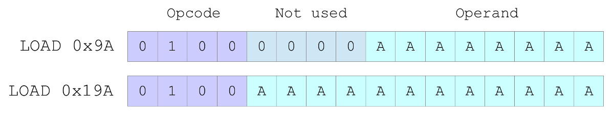
Figure 3 : new absolute addressing mode format
In version 1a of the processor, bits 11 to 8 were unused i.e. were zero, so we can use this space to store the high nibble of the 12bit address, without affecting the instruction's encoding. To further increase the processor's address range e.g. 65536 memory locations, would require a 16bit address therefore, a shift to a 20bit instruction (4bit opcode + 16bit address), making the two processors incompatible. This upgrade does come with an associated increase in memory costs, however, you only need to add as much memory as required i.e. you don't need to add the full 4K. However, a hidden internal cost comes with the increase in hardware associated with the address multiplexer and program counter. The logic, adder and registers associated with these components needs to be increased in size from 8bit to 12bit i.e. 33% increase in hardware requirements.
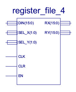
Figure 4 : register file symbol.
The main advantage of an accumulator based architecture i.e. a system with only one general purpose register (GPR), is that you don't need to encode (within an instruction) where one of the operands is coming from or where the result will be stored, as its implicit, it must be the accumulator. This helps reduce the number of bits needed to encode an instruction and helps reduce hardware costs: only one GPR, so less flip-flops and we can hard-wire some parts of the system i.e. reduce the number of MUXs. The main disadvantage of an accumulator based architecture is that everything has to go through the accumulator i.e. its tricky to store variables on the processor, as each instruction tends to want to overwrite it. Therefore, variables are stored in memory, as a result we need a lot more LOAD/STORE instructions to process this data, significantly reducing processing performance i.e. longer program = slower execution time. This further hits processing performance if memory is slower than the processor i.e. can the processor get the data it needs when it needs it, or does it need to wait. Therefore, the number of general purpose registers is increased to four. This "array" of registers is referred to as a register file. The new and improved hardware is shown in figure 5, having four general purpose registers: RA, RB, RC and RD.
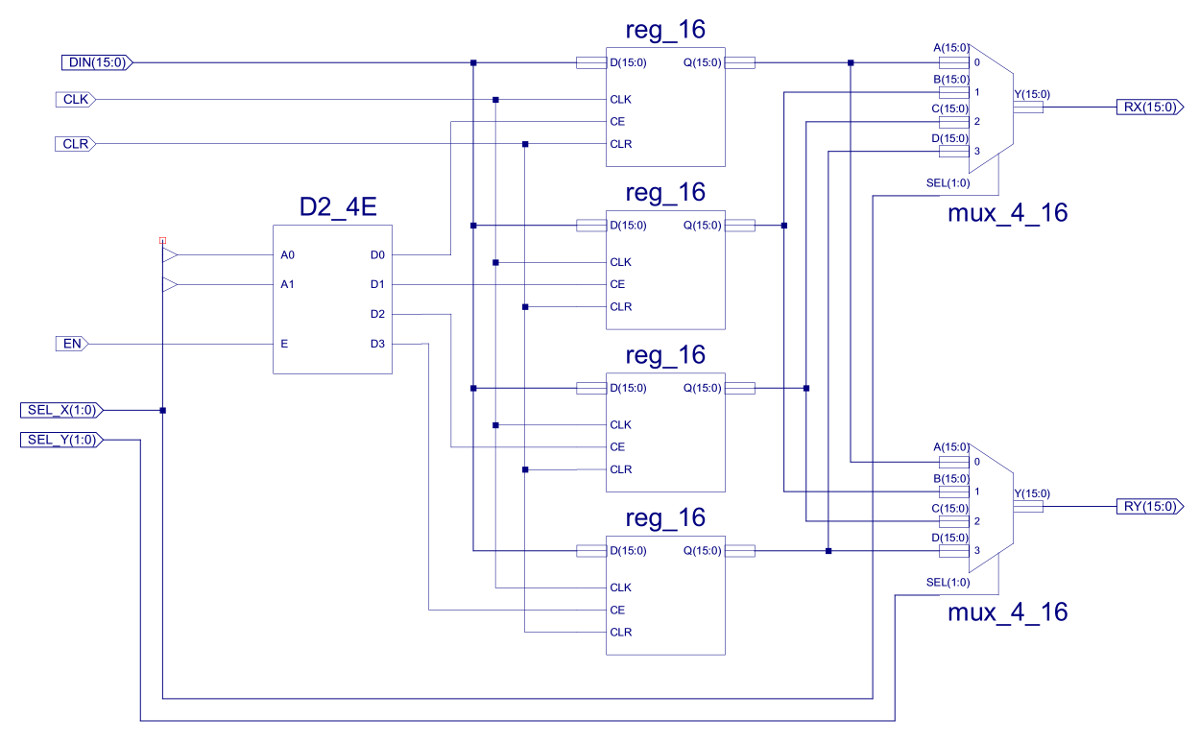
Figure 5 : register file.
The width of the GPRs has also been increased from 8bits to 16bits. The main reason for this change was due to the intended application domain i.e. need to represent values larger than 255, but also due to the previous improvement e.g. if we need to store the value of an address in a register, we now need to store a 12bit value. From an implementation point of view this new component is made from existing components, except for the D2_4E. This is from the Xilinx component library, a 2bit binary to 4bit onehot decoder.
Note, this register file has one write port and two read ports i.e. we can write one value and read two values in parallel. The functionality to read two values at the same time is not required by the previous supported addressing modes, but will be in the new addressing modes discussed later.
The move to multiple GPRs means that an operand source and result destination are no longer implicit, therefore, we need extra bit fields within the instruction, as shown in figure 6. These bit fields identify the register being used, therefore, as we have four registers to select from we will need 2bits.
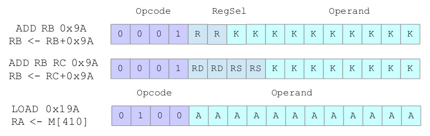
Figure 6 : possible register instruction encoding
For some instructions e.g. immediate ADD, there are number of different choices on how we encode this information. We could go for a two operand format, using a common two bit bitfield: R, to encode one operand's source and the result's destination. Alternatively, we could use a three operand format, using two, two bit bitfields: RD and RS, to separately encode the result's destination (RD) and one operand's source (RS) i.e. maximise flexibility.
Note, always remember that "flexibility" normally comes at a hardware cost i.e. we will need additional multiplexers to select which register should be read or written to. Hard-coding source / destination registers allows the hardware to be hard-wired.
For some instructions this flexibility is not possible, consider the LOAD instruction shown in figure 6. There is no space to encode which of the four registers the data read from memory should be stored in. Therefore, we have to hardcode this into the instruction i.e. any instructions that use the absolute addressing mode must use register RA.
Another ripple caused by the inclusion of the register file is its affect on the flow control instruction group i.e. the previous processor conditional JUMP instructions were based on the ACC state, now we have a choice, which register should be tested? Solution : use a status register. This records the outcome of the last arithmetic or logical function performed, control instructions are now based on this, rather than specific registers. To further improve functionality and to simplify programming we can also add new status bits:
This improvement has a significant impact on hardware requirements e.g. the move from an 8bit ripple adder to 16bits will double hardware requirements. Another, perhaps less obvious impact is upon how the processor is programmed. Consider the instructions shown in figure 7.
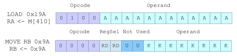
Figure 7 : initialising a register problem
Note, we could of defined a 10bit immediate value in the MOVE instructions, however, i decided to keep with an 8bit value and have two unused bits i.e. "U" bits. No hard reasons, but wanted to keep data aligned to 8bit boundaries.
There are two ways of initialising the value stored in a register, you can either load this value from memory (absolute addressing) or move a value into it (immediate addressing). The LOAD instructions functionality is actually simplified by the move to a 16bit registers i.e. we no longer waste half our memory when we store a variable. However, we do now have an issue with the MOVE instructions. As shown in figure 7 we can only specify an 8bit immediate value. We can "initialise" a register with an 16bit value, if that value is 8bits i.e. we can sign extend as shown in figure 8.
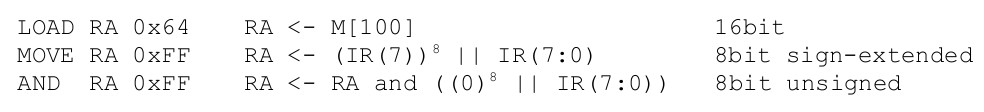
Figure 8 : sign extension
As discussed above LOAD instruction is unaffected. For arithmetic instructions (ADD/SUB) we can treat the 8bit immediate as a signed value, replicating the MSD of this number i.e. bit7, eight times to generate an 16bit signed value. For logical instructions (AND) there is no concept of sign i.e. the operands are just bit patterns, therefore, we pad the high byte with 0's to produce a 16bit value.
This gets around some of these initialisation problems, but we may still need to load a 12bit address, or a full 16bit value. Given the current set of instructions this is not possible. One solution would be to move away from a fixed length (16bit) instruction format, to a variable length instruction. Now an instruction can be as long as we need, being stored across multiple memory locations e.g. we can store the opcode and perhaps an immediate values in one memory location and the address in the next to produce an 32bit instruction. Although possible, this approach does come at a hardware cost i.e. adds complexity to the FETCH phase as we now have a program made up of 16bit and 32bit instructions i.e. how many memory locations should be read in the fetch phase, 1 or 2, what is the PC incremented by? In these situations a common approach taken in processor design is to ask the question: how often do we do this. If the answer is "not that often" then rather than adding additional hardware or instructions we try to implement this functionality using multiple machine-level instructions. Consider the instructions in figure 9.
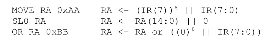
Figure 9 : initialising a 16bit register
Using these instruction we could initialise a register to any value e.g. 0xAAAA, code shown below:
CODE                REGISTER RA
----                -----------
move RA 0xAA          0xFFAA
sl0 RA                0xFF54
sl0 RA                0xFEA8
sl0 RA                0xFD50
sl0 RA                0xFAA0
sl0 RA                0xF540
sl0 RA                0xEA80
sl0 RA                0xD500
sl0 RA                0xAA00
or RA 0xAA            0xAAAA
Alternatively, if we don't have space to add these new instructions we can perform implement the same functionality using the instructions in figure 10. This is a less efficient implementation, so does come with a bit of a performance hit. Also, we still need to add one instruction e.g. an unsigned ADD (addu), to simplify the process of updating the lower byte. However, if pushed this could also be removed, loading this value via an indirect method e.g. if we want to load the value 10 we could perform the addtion of 5+5.
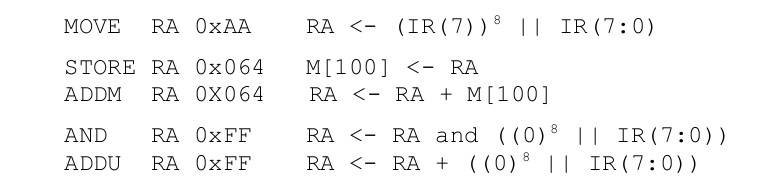
Figure 10 : initialising a 16bit register, alternative solution
CODE                REGISTER RA
----                -----------
move RA 0xFF          0xFFAA
store RA tmp
addm RA tmp           0xFF54
store RA tmp
addm RA tmp           0xFEA8
store RA tmp
addm RA tmp           0xFD50
store RA tmp
addm RA tmp           0xFAA0
store RA tmp
addm RA tmp           0xF540
store RA tmp
addm RA tmp           0xEA80
store RA tmp
addm RA tmp           0xD500
store RA tmp
addm RA tmp           0xAA00
store RA tmp
addu RA 0xAA          0xAAAA
If this functionality is only used to initialise variables at the start of a program the performance hit i.e. the 8 shift instructions, isn't so bad. However, to help reduce these overheads further we could define a "shift left by eight positions" instruction, alternatively, we could consider adding a bit more hardware and add a barrel shifter: (Link).
With the addition of more general purpose registers we can now implement two new addressing modes:
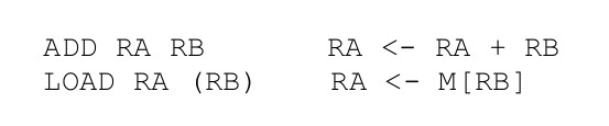
Figure 11 : new register based addressing mode
The main advantages of these addressing modes is that they reduces the need to store variables in memory i.e. removes LOAD/STORE instructions, increasing performance. Less instruction in a program = quicker execution time. They also remove the need to use self-modifying code as we can use registers as pointers i.e. store the address in memory of the data we want to use in a GPR, rather than using the absolute addressing mode, hard-coded in the instruction.
A side affect of the these two new addressing modes is that we now no longer need to define a "number" within the instruction i.e. an immediate value or an address. This free's up 8bits within the instruction that can be re-purposed. A very common optimisation is to use this space to expand the opcode field, allowing the processor to define more machine-level instructions. Therefore, we can use the same "opcode" for each "register based" instruction, then use the lower nibble to identify the type of register based instruction to perform, as shown in figure 12.
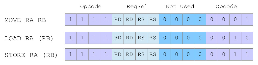
Figure 12 : register based addressing mode encoding
For the simpleCPU the top opcode field is set to "1111", the lower opcode field is then decoded to identify what register based instruction should be performed. This leaves 8bits to define operand source and result destination. To keep things simple a 2-operand format was selected for the simpleCPUv1d, however, there are no reasons why other encodings could not be used, some examples are shown in figure 13.
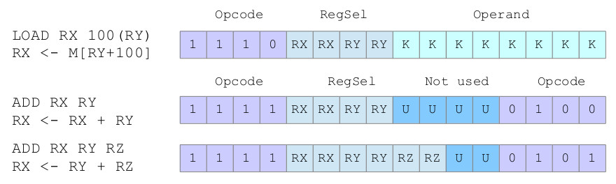
Figure 13 : alternative encodings
We could also implement the displacement addressing mode as illustrated by the LOAD instruction. Here the base address stored in register RY is "displaced" by the immediate data KK to generate the actual address. This address is generated at runtime so an additional adder would be required. This example defines the opcode in the top nibble, we could implement this type of functionality using the top/lower opcode format, however, this would limit the displacement to a 4bit value, which may be a little limiting. Again to add more flexibility to the register addressing mode we could specify different source and destination registers. This has the advantage that we do not have to overwrite one of the operands as for the 2-operand format instructions. Note, RX and RY can be any register i.e. RA, RB, RC or RD. As always this flexibility helps reduce the number of instructions needed to implement a program, helping to increase processing performance, but it comes at a hardware cost.
Note, this is your classic CISC (Link) and RISC (Link) trade-off i.e. is it better to increase instruction functionality and reduce the number of instructions needed by a program, or is it better to simplify the instructions, minimising hardware back to its absolute basics in an effort to reduce the critical path delay, allowing you to clock the hardware faster, compensating for the increased instruction count? There is no right or wrong answer here, it all depends on the system's bottlenecks and the applications you are performing.
To simplify coding the processor needs to support the software programming constructs used by the programmer i.e. we need to match the high level representations to low level implementations. Therefore, we need to support some sort of function call i.e. a write once use many times coding structure. In version 1a we implemented this functionality using a mixture of macros and self-modifying code e.g. the Wheeler Jump. These are both powerful ideas, but as previously discussed these do have fundamental disadvantages. A subroutine, commonly referred to as a: routine, procedure, function, or method, is a block of code that can be written once and then “called” from anywhere in a program, as shown in figure 14.
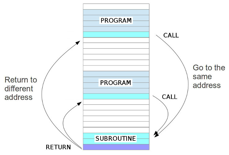
Figure 14 : subroutines
To implement this within the processor we need two more instructions:

Figure 15 : CALL / RET instructions
The RTL discriptions for these instructions are given below:
CALL AA                     RET
-------                     ---
M[SP] <- PC+1               SP    <- SP-1
SP    <- SP+1               PC    <- M[SP]
PC    <- AA
The CALL instruction is comparable to a JUMP, but with the additional feature of remembering the address it has to jump back to after it has completed the subroutine. This information is stored on a stack. Each time a subroutine is called its return address is pushed onto the stack i.e. a subroutine can CALL another subroutine, or itself if we are using recursive programming. The RET instruction pops off the last address pushed onto the stack, updating the program counter with this return address. To organise the stack we need a stack pointer (SP), a register that points to the next free memory location on the stack. However, to add a little variety i've implemented this stack in a separate block of hardware, rather than external memory, as shown in figure 16.
Note, this method of implementing the stack is a little different than that used in normal processors, but is not unknown e.g. Xilinx's PicoBlaze processor, i have also implemented the CALL/RET instructions using the more classical POP/PUSH instructions, discussed later...
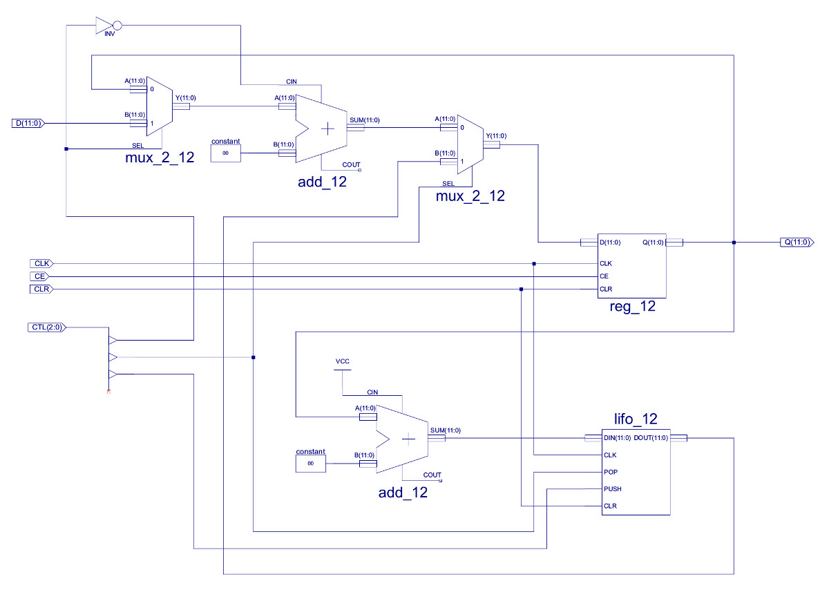
Figure 16 : updated program counter (PC)
This version of the PC has been upgraded from 8bits to 12bits to support the move to a 4K memory space. In addition to this, in the bottom half of the schematic ive added a hardware LIFO i.e a Last In First Out buffer. The input data to this component is the current PC+1, the output being used as an input source for the PC register. The LIFO's symbol is shown below:
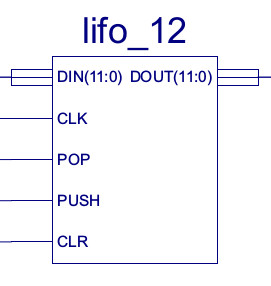
Figure 17 : LIFO symbol
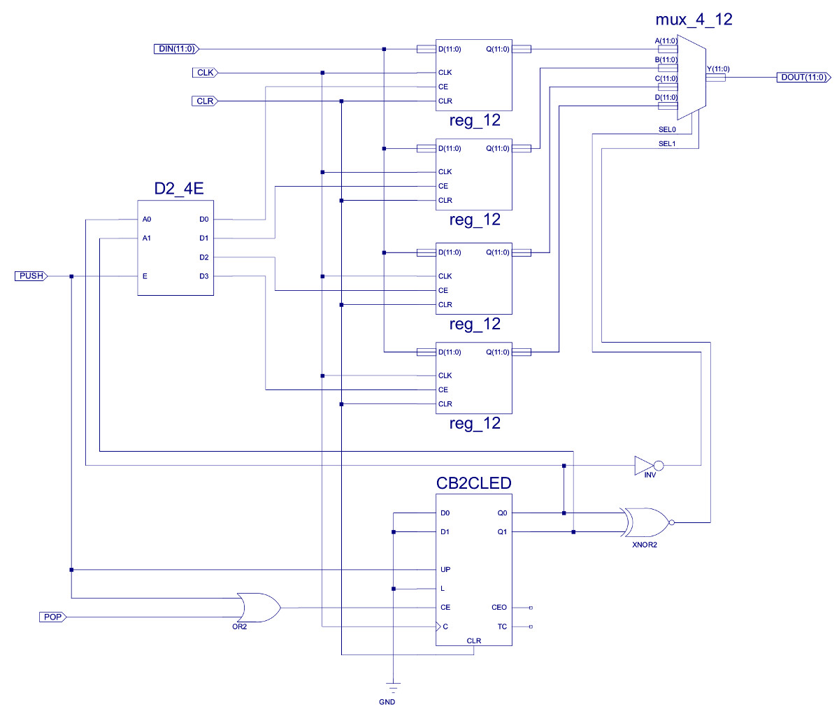
Figure 17 : LIFO - last in, first out buffer
The LIFO_12 component is made from four 12bit registers (REG_12) that implement its "memory". A two bit binary counter (CB2CLED) that implements the stack pointer, combined with a decrementer (XNOR+INV) and a 2-4 onehot decoder (D2_4E) that control pop/push operations to this memory (stack). Finally, to select the top of stack value a four input 12bit output MUX (MUX_4_12) is used. In operation the counter's output is decoded by the onehot decoder, enabling the next free register (WR_PNTR), the decremented current count value controls the output multiplexer, selecting the last pushed value (RD_PNTR). To better understand this components operation consider the code shown in figure 18.
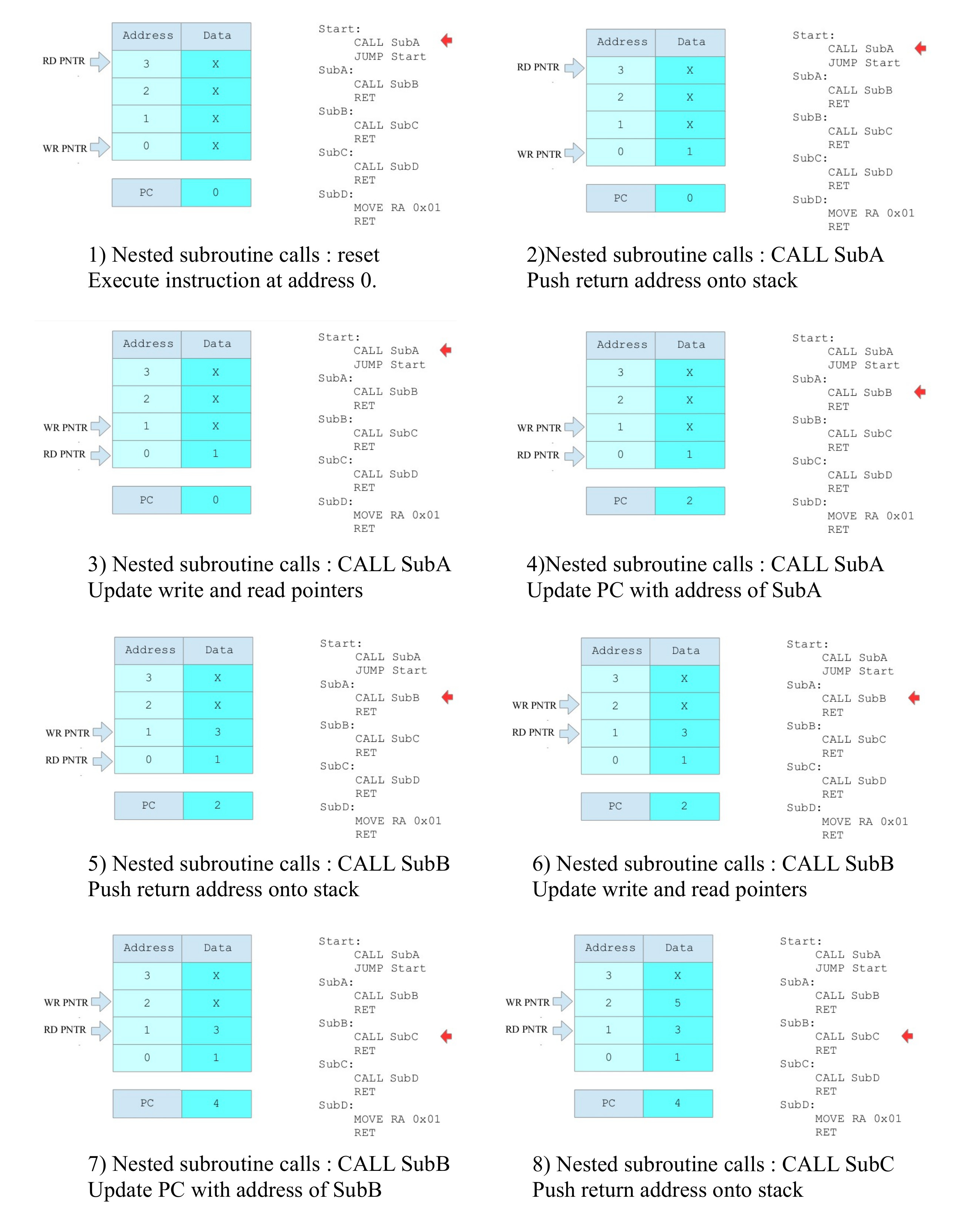
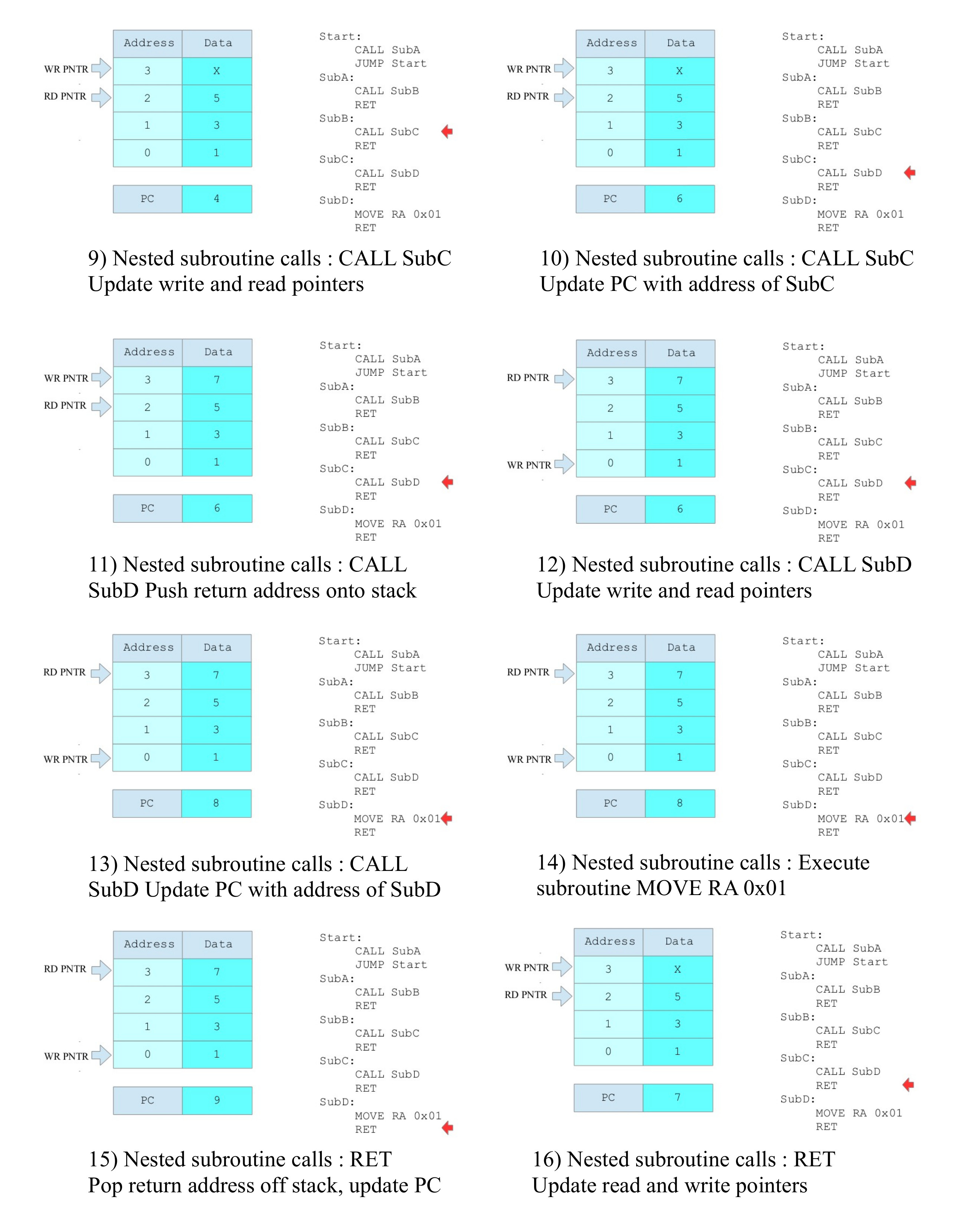
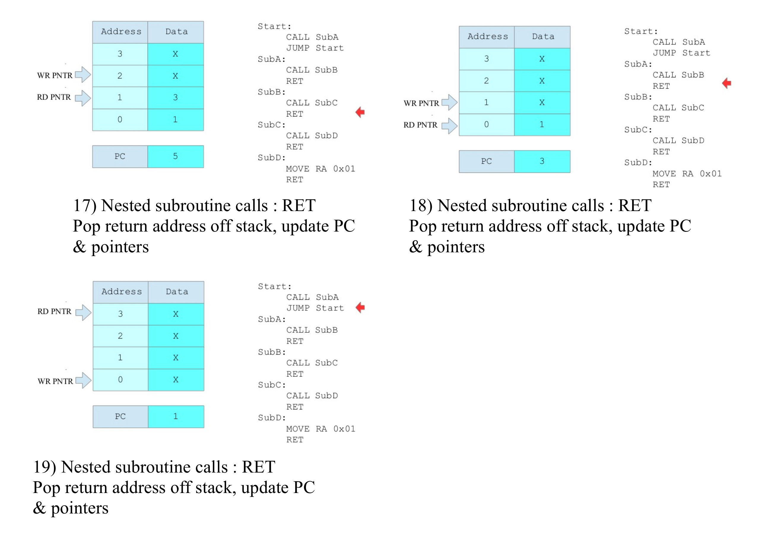
Figure 18 : example stack CALL/RET code
Initially the stack pointer is zero, therefore, the write pointer WR_PNTR=0 and the read pointer RD_PNTR=-1. At present there is no error detection in the stack, so if a pop whilst empty is performed the PC will be updated with rubbish. When a push operation is performed the register addressed by the WR_PNTR is updated, then the counter is incremented. As the RD_PNTR=WR_PNTR-1 the output MUX selects the data at the last pushed address. Each time a push operation is performed the next free register is updated and the binary counter is incremented. Again, there is no error detection in the stack, if a push whilst full is performed, this will overwrite a previously stored return address. Therefore, a maximum of four nested subroutine calls can be performed.
Note, unlike some processor's parameters that will be used by the subroutine can not be pushed onto this stack i.e. the stack only contains the return address. Therefore, parameters must be passed using a separate software controlled data stack implemented in external memory, specific hard-coded memory locations, or registers. To highlight these differences the more "classical" method of using a stack and frame pointer will be added / discussed later.
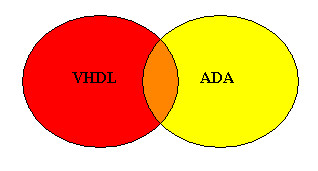
Figure 19 : Ada=SW and VHDL=HW
The improvement to the control logic is in its implementation, a switch from schematic to a hardware description language (HDL). The simpleCPU processor was developed using the Xilinx ISE tools so that we can use schematics. From a teaching point of view this visual representation is far superior than HDLs i.e. the conceptual gap from block diagram to schematic is very small, allowing you to see the path from design to implementation. The downside of schematics is the time it takes to draw them. Even though the SimpleCPU is a very small piece of hardware it does take a long time to layout and draw each circuit. Therefore, to simplify the construction of the control logic i moved to and HDL, as the VHDL syntax used in the construction of this component (simple combinatorial logic) is very similar to the RTL descriptions used to define the processor's micro-instructions. VHDL is a double acronym:
This language was commissioned by the American Department of Defense in the early 1980’s as an implementation independent method of describing electronic systems, being based on their software programming language Ada. As i had programmed in Ada for many years this was a natural switch for me, but other HDLs are available. VHDL was primarily designed as a hardware modelling / specification language. Used in all stages of design, from system level modelling of the specification, down to modelling timing characteristics of implemented systems. A key feature of this language is the automated synthesis tools, used to convert VHDL descriptions into ICs i.e. tools construct and optimize a gate level design from abstract RTL descriptions, significantly reducing hardware development and testing times.
The smallest item that can be compiled in VHDL is a design unit, these are:
To illustrate how these units are used consider the AND gate shown in figure 20.
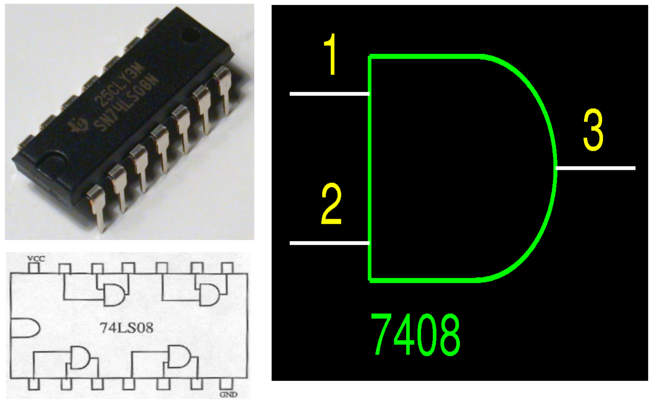
Figure 20 : 7804 AND gate
The AND gate's input and output pins (ports) are defined in the component's entity, given the user defined name "AND_GATE", as shown in figure 21. This unit defines each pins:
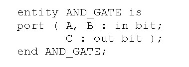
Figure 21 : VHDL entity
An entity declares a components interface, its functionality is declared in its architecture, given the user defined name "AND_GATE_ARCH" linked to the entity name "AND_GATE" as shown in figure 22.
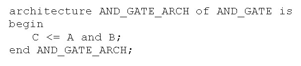
Figure 22 : VHDL architecture
The required logic function is defined using a simple concurrent signal assignment "<=" i.e. the result of A and B drives the output C. A very similar syntax to the RTL syntax used to define the machine's micro-instructions. VHDL supports the following logical operators: NOT, AND, OR, XOR, NAND and NOR.
By default VHDL supports a range of built in data types e.g. bit - logic 0 or logic 1. However, to simulate more real world scenarios e.g. a logic 1 and a logic 0 accidentally connected to the same wire, we tend to use the stdlogic data type i.e. multi-valued logic, as shown in figure 23.
Note, as the bit data type can only represent 0 or 1, the short circuit scenario can not be tested for i.e. it has to display a 0 or a 1 in the waveform trace. If we use stdlogic this bad scenario would be resolved to an X i.e. unknown state, displayed in red in the simulation waveform.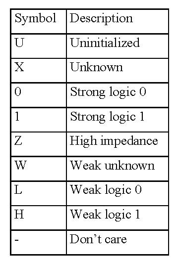
Figure 23 : stdlogic - multi-valued logic
To allow a VHDL component to use this data type we must include the library (package) IEEE.STD_LOGIC_1164 at the start of the file, as show in figure 24. This type definition is contained in the package std_logic_1164 and defines new data types to replace type bits: std_logic and std_logic_vector.
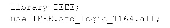
Figure 24 : IEEE STDLOGIC library
The finished AND gate, its testbench and resulting simulations are shown in figure 25.
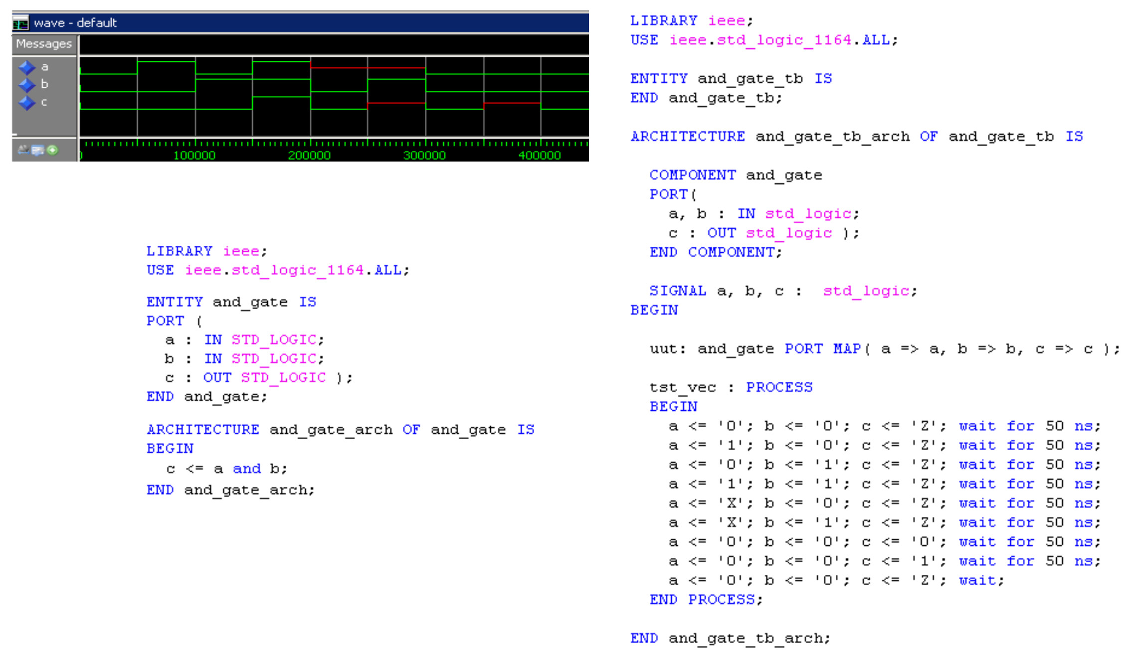
Figure 25 : AND gate, testbench and simulation
Generation of the final control logic is identical to the process described for the simpleCPU_v1a processor. The top level control logic symbol and schematic are shown in figures 26 and 27.
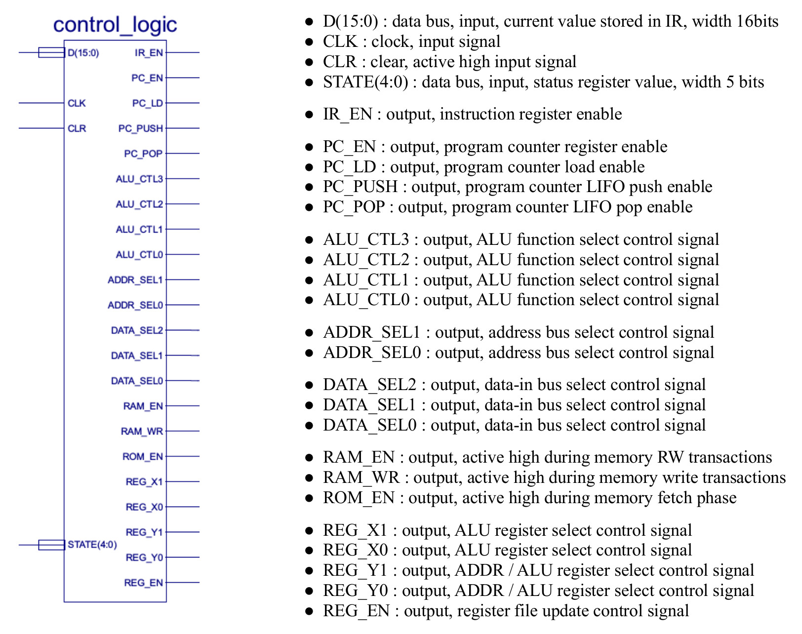
Figure 26 : Control logic symbol
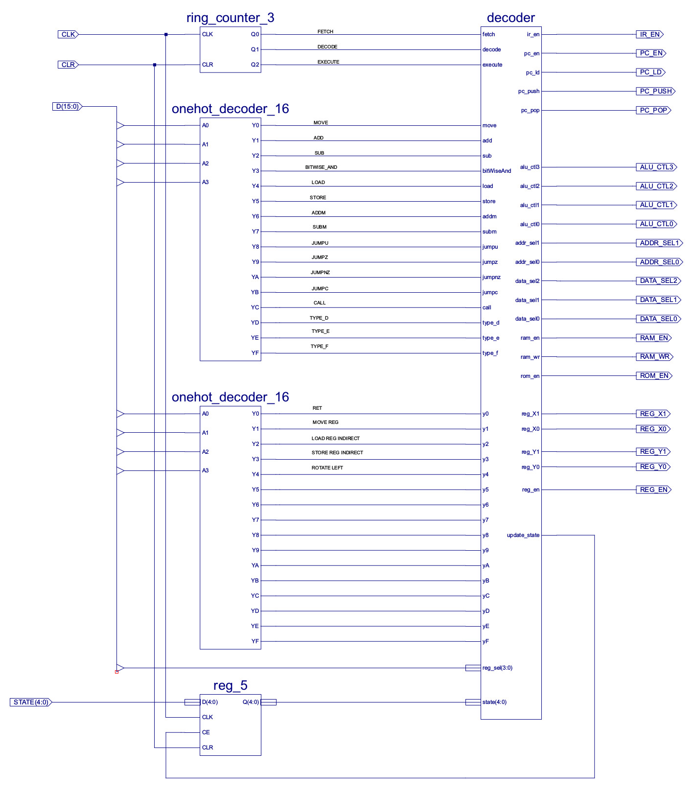
Figure 27 : Control logic schematic
The control logic uses the same ring counter and onehot decoder as before. An additional onehot decoder is added for register based instructions i.e. type_f, top opcode value "1111", decoding the lower nibble. The status register is also included in this component (bottom left), a five bit register storing the status of the last ALU operation. The status register bits (flags) are:
These status bits are generated within the ALU and its adder-subtracter unit. The Zero flag is generated using a 16bit NOR gate connected to the output of the ALU. The Carry flag is the MSB carry out (COUT) of the ripple adder, with a small twist, as subtraction is performed through the addition of a negative number, this COUT is ANDed with the inverse of ALU_CTL0. This disables the Carry flag during subtract operations i.e. the final COUT of signed arithmetic is normally ignored. The Overflow flag is generated using the XOR network shown in figure 29, comparing the MSB of the result and operands. The XNOR tests to see if the operand sign bits are the same, if so the MSB of the result and operand A are compare, if there is a mismatch an overflow has occurred. The Positive and Negative flags are simply based on the MSB of the ALU output i.e. P=NOT(ALU(15)) and N=ALU(15).
Note, at present only the Zero flag is used e.g. JUMPZ, but its a simple job to add more conditional jump instructions or other instructions, opcode space allowing.
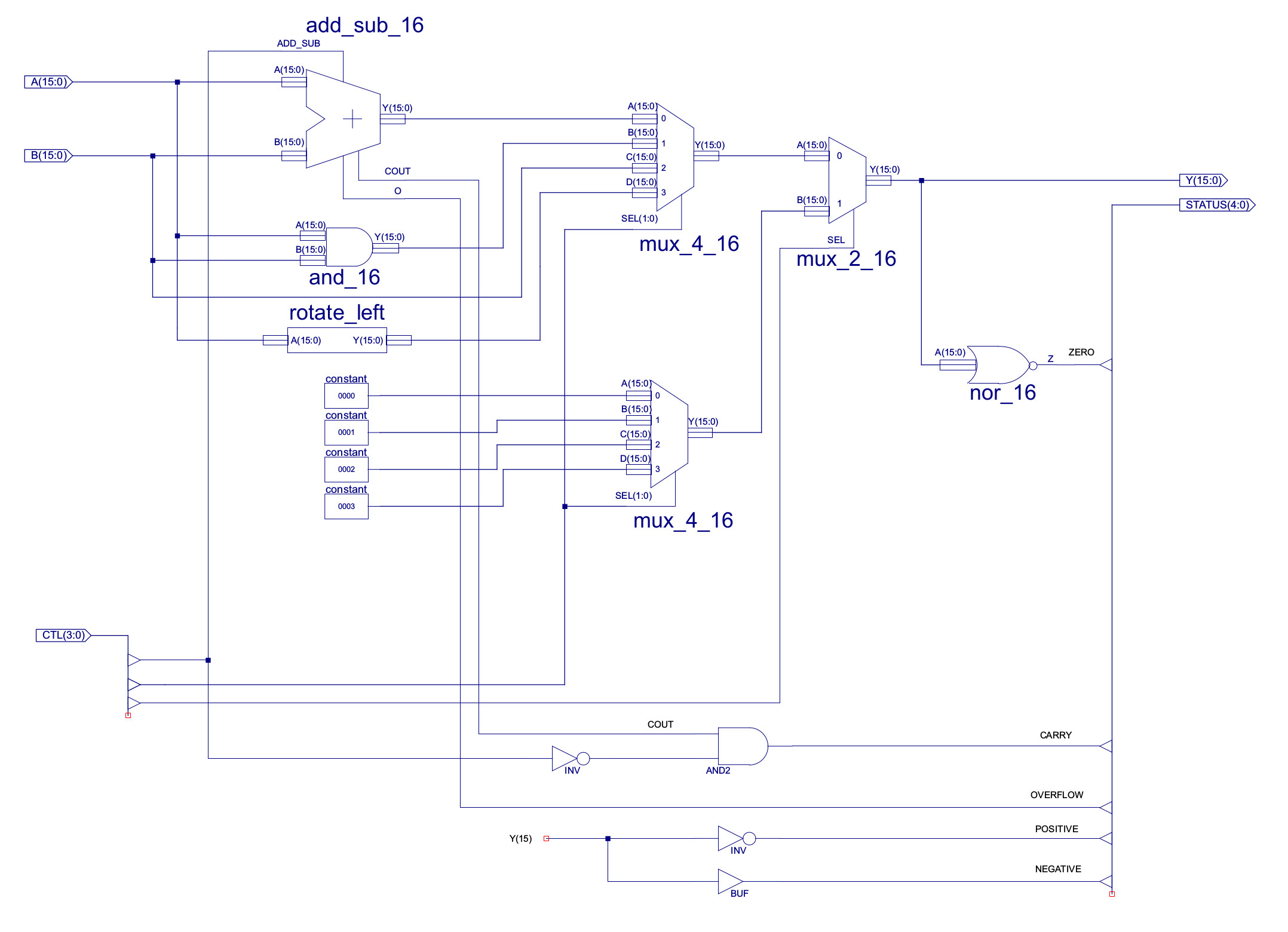
Figure 28 : ALU
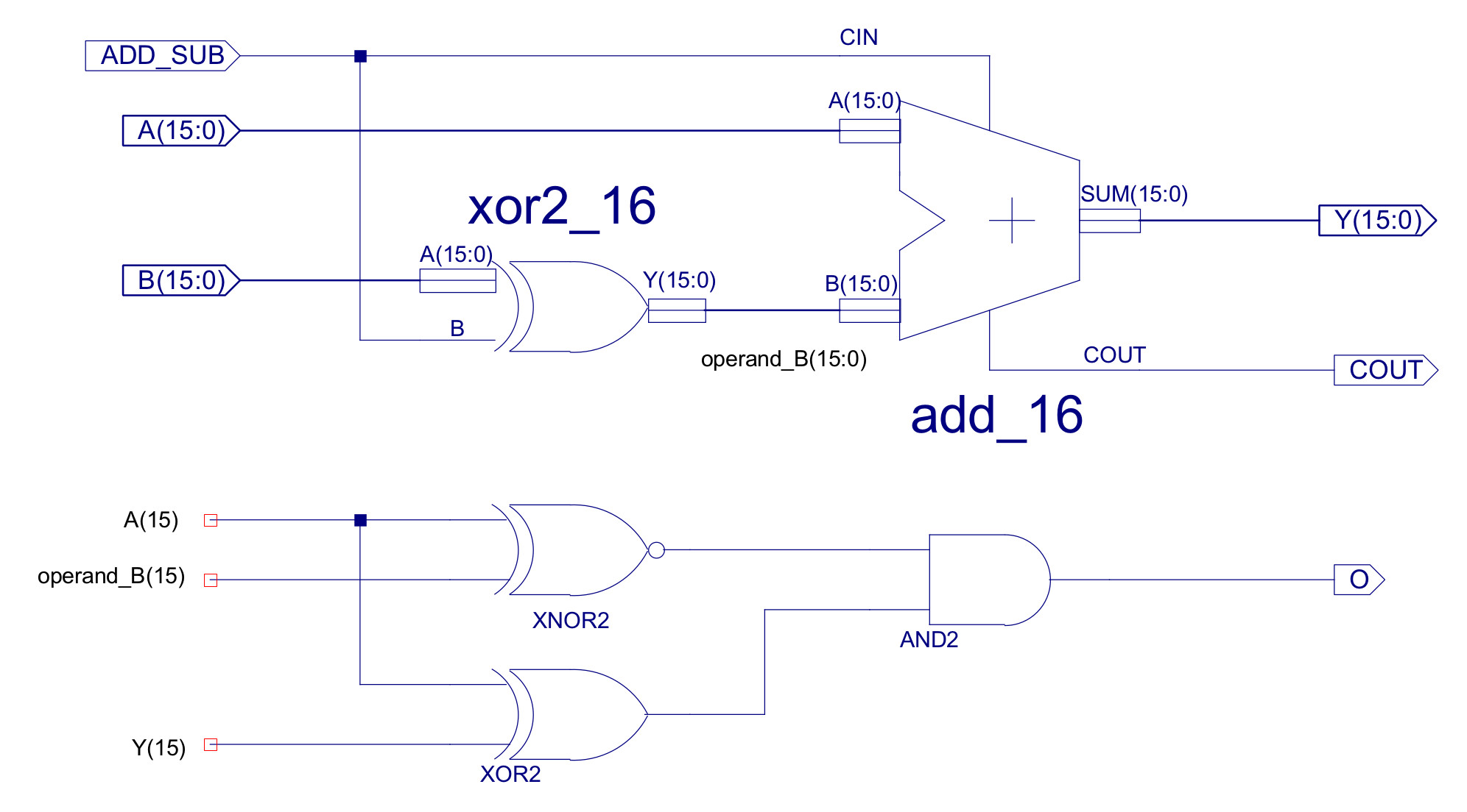
Figure 29 : adder subtractor unit
The final VHDL control logic is shown in figure 30.
----------------------------------------------------------------------------------
-- Create Date:    19:09:28 01/08/2020
-- Module Name:    decoder

-- Revision 0.01 - File Created
-- Additional Comments:
--
----------------------------------------------------------------------------------
library IEEE;
use IEEE.STD_LOGIC_1164.ALL;

entity decoder is
Port (
  fetch          : in  STD_LOGIC;
  decode         : in  STD_LOGIC;
  execute        : in  STD_LOGIC;

  state          : in  STD_LOGIC_VECTOR(4 DOWNTO 0);
  reg_sel        : in  STD_LOGIC_VECTOR(3 DOWNTO 0);

  move           : in  STD_LOGIC;
  add            : in  STD_LOGIC;
  sub            : in  STD_LOGIC;
  bitWiseAnd     : in  STD_LOGIC;

  load           : in  STD_LOGIC;
  store          : in  STD_LOGIC;
  addm           : in  STD_LOGIC;
  subm           : in  STD_LOGIC;

  jumpu          : in  STD_LOGIC;
  jumpz          : in  STD_LOGIC;
  jumpnz         : in  STD_LOGIC;
  jumpc          : in  STD_LOGIC;
  call           : in  STD_LOGIC;

  type_d         : in  STD_LOGIC;
  type_e         : in  STD_LOGIC;
  type_f         : in  STD_LOGIC;

  y0             : in  STD_LOGIC;
  y1             : in  STD_LOGIC;
  y2             : in  STD_LOGIC;
  y3             : in  STD_LOGIC;
  y4             : in  STD_LOGIC;
  y5             : in  STD_LOGIC;
  y6             : in  STD_LOGIC;
  y7             : in  STD_LOGIC;
  y8             : in  STD_LOGIC;
  y9             : in  STD_LOGIC;
  yA             : in  STD_LOGIC;
  yB             : in  STD_LOGIC;
  yC             : in  STD_LOGIC;
  yD             : in  STD_LOGIC;
  yE             : in  STD_LOGIC;
  yF             : in  STD_LOGIC;

  ir_en          : out STD_LOGIC;

  pc_en          : out STD_LOGIC;
  pc_ld          : out STD_LOGIC;
  pc_push        : out STD_LOGIC;
  pc_pop         : out STD_LOGIC;

  reg_X1         : out STD_LOGIC;
  reg_X0         : out STD_LOGIC;
  reg_Y1         : out STD_LOGIC;
  reg_Y0         : out STD_LOGIC;
  reg_en         : out STD_LOGIC;

  alu_ctl3       : out STD_LOGIC;
  alu_ctl2       : out STD_LOGIC;
  alu_ctl1       : out STD_LOGIC;
  alu_ctl0       : out STD_LOGIC;

  addr_sel1      : out STD_LOGIC;
  addr_sel0      : out STD_LOGIC;

  data_sel2      : out STD_LOGIC;
  data_sel1      : out STD_LOGIC;
  data_sel0      : out STD_LOGIC;

  ram_en         : out STD_LOGIC;
  ram_wr         : out STD_LOGIC;
  rom_en         : out STD_LOGIC;

  update_state	: out STD_LOGIC );
end decoder;

architecture decoder_arch of decoder is

  signal zero           : STD_LOGIC;
  signal carry          : STD_LOGIC;
  signal overflow       : STD_LOGIC;
  signal pos            : STD_LOGIC;
  signal neg            : STD_LOGIC;

  signal jump           : STD_LOGIC;
  signal write_mem      : STD_LOGIC;

  signal ret            : STD_LOGIC;
  signal move_reg       : STD_LOGIC;
  signal load_indirect  : STD_LOGIC;
  signal store_indirect : STD_LOGIC;

  signal rotate_left : STD_LOGIC;

begin

  -- map state input bus to status bits

  zero     <= state(0);
  carry    <= state(1);
  overflow <= state(2);
  pos      <= state(3);
  neg      <= state(4);

  -- combine high (type_f) and low (Y0-YF) onehot decoder outputs to generate
  -- zero operand / register / register indirect instruction ctl lines

  ret            <= type_f and y0;
  move_reg       <= type_f and y1;
  load_indirect  <= type_f and y2;
  store_indirect <= type_f and y3;

  rotate_left    <= type_f and y4;

  -- interal logic

  jump           <= ( jumpu or (jumpz and zero) or (jumpnz and not zero) or (jumpc and carry) or call or ret);
  write_mem      <= store or store_indirect;

  -- external logic

  ir_en          <= fetch;

  pc_en          <= (decode and (not jump)) or (execute and jump);
  pc_ld          <= execute and jump;
  pc_push        <= decode and call;
  pc_pop         <= execute and ret;

  reg_X1         <= reg_sel(3) and (not store);
  reg_X0         <= reg_sel(2) and (not store);

  reg_Y1         <= reg_sel(1);
  reg_Y0         <= reg_sel(0);

  reg_en         <= execute and (move or load or add or sub or bitWiseAND or
                                 addm or subm or
								 move_reg or load_indirect or rotate_left);

  -- SEL3 SEL2 SEL1 SEL0
  --  0    0    0    0     ADD
  --  0    0    0    1     SUB
  --  0    0    1    X     AND
  --  0    1    0    X     PASS B
  --  0    1    1    X     ROL
  --  1    0    0    X     NU
  --  1    0    1    X     NU
  --  1    1    0    X     NU
  --  1    1    1    X     NU

  alu_ctl3       <= '0';
  alu_ctl2       <= move or load or move_reg or load_indirect or rotate_left;
  alu_ctl1       <= bitWiseAND or rotate_left;
  alu_ctl0       <= sub or subm;

  -- SEL1 SEL0
  --  0   0     PC
  --  0   1     IR
  --  1   0     Register File
  --  1   1     NU

  addr_sel1      <= (decode or execute) and (load_indirect or store_indirect);
  addr_sel0      <= (decode or execute) and (load or store or addm or subm);

  -- SEL2 SEL1 SEL0
  --  0   0    0     IR 8bit unsigned
  --  1   0    0     IR 8bit sign extended
  --  X   0    1     IR 12bit unsigned
  --  X   1    0     DATA-BUS-IN 16bit
  --  X   1    1     RY 16bit

  data_sel2      <= not(bitWiseAND);
  data_sel1      <= load or addm or subm or load_indirect or move_reg;
  data_sel0      <= move_reg;

  ram_en         <= (decode or execute) and (load or store or addm or subm or load_indirect or store_indirect);
  ram_wr         <= execute and (store or store_indirect);
  rom_en         <= fetch;

  update_state   <= execute and (add or sub or bitWiseAND or addm or subm);

end decoder_arch;
Figure 30 : decoder control logic
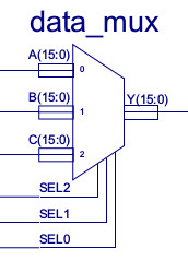
Figure 31 : data MUX symbol
As discussed in section 2 (Improvement 2 : increase internal memory size and width) the processor may have to sign extend immediate values stored in the instruction register. To keep the top level schematic neat and tidy i decided to place this functionality into the data multiplexer, as shown in figure 31.
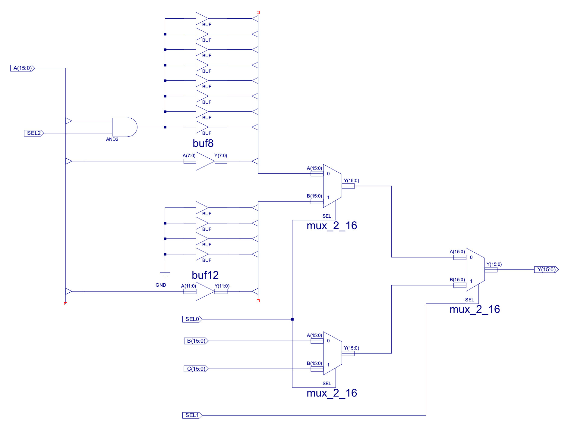
Figure 31 : data MUX
Do confess looking back at this now, perhaps a little over engineered, could be simpler. I'm guessing i was trying to keep things as flexible as possible i.e. to allow different types to addressing modes / instructions etc. The A input of the MUX is driven by the IR i.e. an immediate data value or a direct address. Depending on the type of instruction i.e. arithmetic or logical, we will need to replicate the sign bit (bit7) or logic 0s. The is performed by and AND gate and control signal SEL2. If this data is an address the second input of the internal MUX_2_16 is padded with four logic 0's to produce a 12bit address. At present this is not used in the processor, could possibly be used later to implement displacement or indexed address, but in its present form not needed, so could be removed. The B and C inputs of the MUX take data from external memory and the register file. As both of these are 16bit value we do not need to sign extend these values.
WORK IN PROGRESS

This work is licensed under a Creative Commons Attribution-NonCommercial-NoDerivatives 4.0 International License.
Contact email: mike@simplecpudesign.com