The minimalCPU was developed as a simplified teaching architecture, a computer designed to introduce assembly language programming to students that had only programmed in high level languages such as python. As such it was never intended that this architecture would be implemented in a hardware, in an FPGA. Therefore, to help student's visualise how these assembly language (machine-level) instructions are executed on this architecture, the animated minimalCPU instruction-set simulator was developed (Link). This combined with the command-line instruction-set simulator allows students to single step through / run minimalCPU programs. However, these lack that impact of flashing LEDs, sooo, i decided to implement this processor in an FPGA. As always its not just a question designing and implementing this hardware, its a question of what does this bring to the table, does this improve the learning experience, or does it just add to the confusion :).
Note, part of the reason for not building the minimalCPU in an FPGA was because designing hardware for an architecture that was never meant to be implemented on an FGPA brings with it a number of implementation joys, sooo this is may take a couple of iterations, or i could get this right first time.
Instruction-set and Assembler
Hardware
Monitor - upload / download code
How to use the minimalCPU in the lab
Quizzz
Before we can think about designing hardware we need to decide how the minimalCPU's machine-level instructions (below) will be represented in hardware i.e. what binary encoding will be used within the processor.
Note, the following ramblings / discussions do assume you understand what a binary number is, sooo, for more info on base-2 numbers have a look here: (Link).
INSTRUCTION      DESCRIPTION                               EXAMPLE

ADD X Y          Perform the ADDITION function on          X = X ADD Y
                 two variables X and Y, storing the        ADD 11011011 00001111
                 result in variable X.
                                                           X = 11011011
                                                           Y = 00001111
                                                               --------
                                                               11101010
                                                               --------
                                                                 11111

ADD X 10         Perform the ADDITION function on          X = X ADD Y
                 variable X and constant 10, storing       ADD 11011011 00001010
                 the result in variable X.
                                                           X = 11011011
                                                           Y = 00001010
                                                               --------
                                                               11100101
                                                               --------
                                                                 11 1

AND X Y          Perform the bitwise AND function on       X = X AND Y
                 two variables X and Y, storing the        AND 11011011 00001111
                 result in variable X.
                                                           X = 11011011
                                                           Y = 00001111
                                                               --------
                                                               00001011
                                                               --------

AND X 10         Perform the bitwise AND function on       X = X AND 10
                 variable X and constant 10, storing       AND 11011011 00001010
                 the result in variable X.
                                                           X = 11011011
                                                           Y = 00001010
                                                               --------
                                                               00001010
                                                               --------

XOR X Y          Perform the bitwise XOR function on       X = X XOR Y
                 two variables X and Y, storing the        XOR 11011011 00001111
                 result in variable X.
                                                           X = 11011011
                                                           Y = 00001111
                                                               --------
                                                               11010100
                                                               --------

XOR X 10         Perform the bitwise XOR function on       X = X XOR 10
                 variable X and constant 10, storing       XOR 11011011 00001010
                 the result in variable X.
                                                           X = 11011011
                                                           Y = 00001010
                                                               --------
                                                               11010001
                                                               --------

OR X Y           Perform the bitwise OR function on        X = X OR Y
                 two variables X and Y, storing the        OR 11011011 00001111
                 result in variable X.
                                                           X = 11011011
                                                           Y = 00001111
                                                               --------
                                                               11011111
                                                               --------

OR X 10          Perform the bitwise OR function on        X = X OR 10
                 variable X and constant 10, storing       OR 11011011 00001010
                 the result in variable X.
                                                           X = 11011011
                                                           Y = 00001010
                                                               --------
                                                               11011011
                                                               --------

JPZ loop         Jump to label "loop" if the last          loop:
                 calculation generated a zero result,         AND Z 0
                 this example implements an infinite          JPZ loop
                 loop i.e. program trapped.
These human readable instructions i.e. ADD, AND, OR, XOR and JPZ, are the processor's assembly language (Link), the words you use to define what functions / operations your program performs. Typically these characters are represented in a file using ASCII codes (Link). Each graphical character is represented by a number e.g. A = 65, when you open this file with Notepad (other text editors available), these numbers are converted into the graphical fonts (Link) that the user can read e.g. code 65 prints "A" to the screen. Consider the characters used to represent the word "ADD":
Char  Dec   Hex    Bin
A     65    0x41   01000001
D     68    0x44   01000100        ADD = 01000001 01000100 01000100
D     68    0x44   01000100
Sooo, within the minimalCPU's hardware we could use the binary code "01000001 01000100 01000100" to represent the operation "ADD" i.e. use this 24bit binary value as its opcode. However, if we take this approach the size of the opcode would vary e.g. ADD = 24bits, OR = 16bits. Also, this encoding is quite sparse, not all combinations of 1s and 0s are used, sooo we are wasting memory, a smaller more compact representation would be more efficient.
The minimalCPU has five basic instructions i.e. ADD, AND, OR, XOR and JPZ, however, four of these instructions have two different variants / formats, process different types of data. The data an instruction processes are called operands, how this data is accessed is called its addressing mode. Consider the ADD instruction:
ADD X Y    -   X = X + Y    - add two variables
ADD Z 123  -   Z = Z + 123  - add a variable and a number
Here, we have two instructions that perform the same function / operation i.e. ADD, but the values they ADD are different i.e. two variables, or a variable and a number. Sooo, even though they are both "ADD" instructions, within the processor we need to give them different opcodes, so that the processor can work out how the data should be accessed, what addressing modes the instruction is using. Therefore, one possible 4bit encoding would be:
Instr              Dec    Bin
ADD VAR VAR    -   0      0000
ADD VAR NUM    -   1      0001
AND VAR VAR    -   2      0010
AND VAR NUM    -   3      0011
XOR VAR VAR    -   4      0100
XOR VAR NUM    -   5      0101
OR  VAR VAR    -   6      0110
OR  VAR NUM    -   7      0111
JPZ ADDR       -   8      1000
Note, nothing complex here, we just need to give each instruction an unique number i.e. the same idea as ASCII, the code for "A" could have been 0, it does not need to be 65, we just need to give each character or opcode a unique value.
The next thing we need to define in the instruction are its operands. Variables (VAR) are given the names / labels A to Z, thats 26 things to identify, sooo, we will need a 5bit value. Numbers (NUM) are 8bit values, this is defined / fixed by the processor's hardware. Typically decided by the types of applications / programs running on the processor, also cost i.e. what range of values does the processor need to process, the bigger the value the more hardware needed to process them, sooo small = cheap.
                             16 8 4 2 1      16 8 4 2 1
VARIABLES A to Z = 0 to 25 = 0  0 0 0 0  to  1  1 0 0 1

                   128 64 32 16 8 4 2 1      128 64 32 16 8 4 2 1
NUMBERS 0 to 255 = 0   0  0  0  0 0 0 0  to  1   1  1  1  1 1 1 1
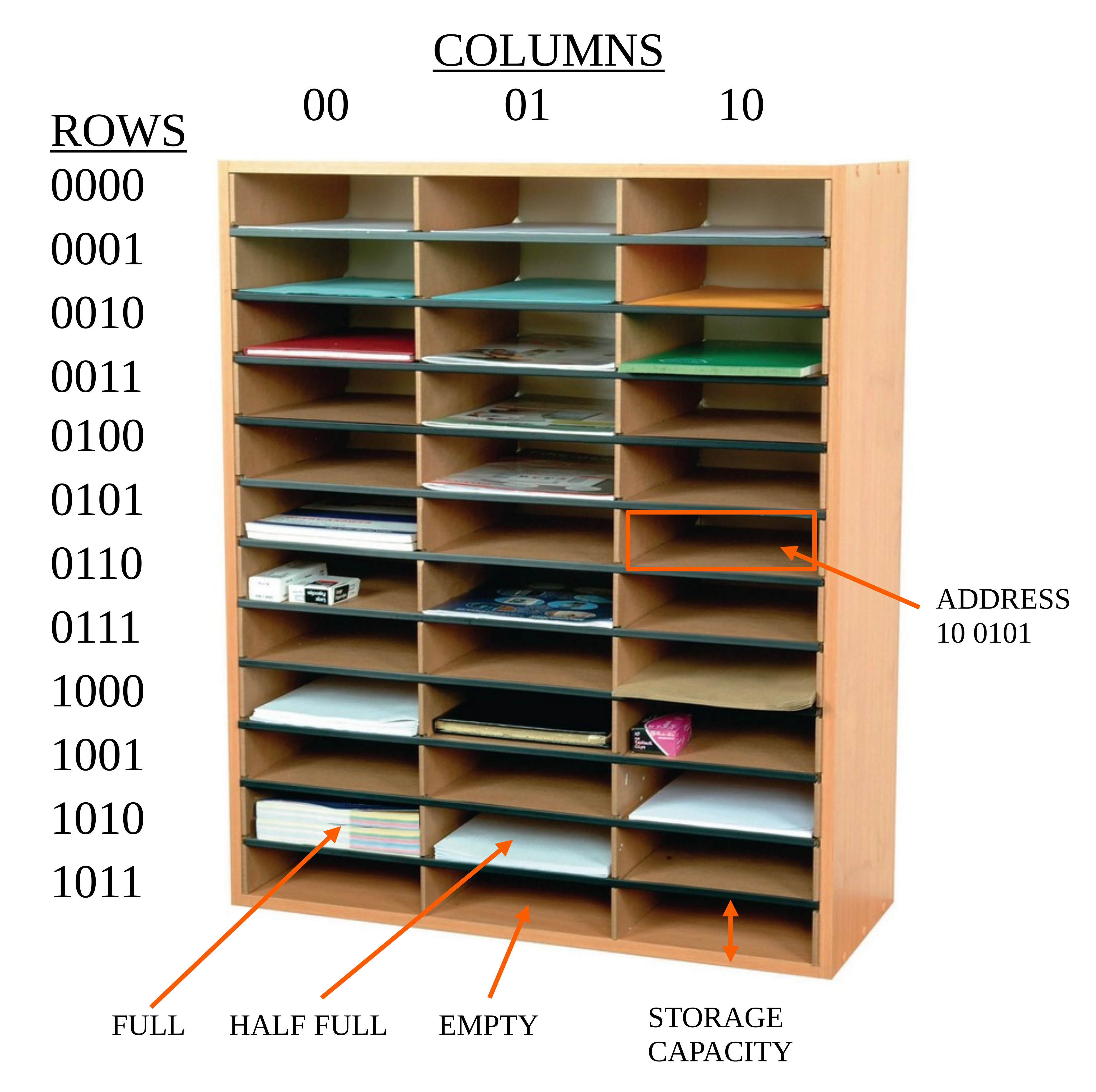
Finally we need to define the operand used by the JPZ instruction i.e. what is a label? This brings in a concept that the minimalCPU ignored: memory (Link). Inside a computer there are lots of different types of memory, but for the moment consider memory as a set of pigeon holes, as shown in figure 1. This set of pigeon holes has 36 storage locations, organised as 12 rows and 3 columns. The location of each pigeon hole i.e. its address, can be defined by its ROW (0000 to 1011) and COLUMN (00 to 10) number e.g. the location on the sixth row in the third column has the address 10 0101, or the decimal value 21. Each storage location has a fixed capacity, you can store different amounts of paper in each location, but storing less in one does not free up more space in others.
Figure 1 : Memory
In the minimalCPU each instruction is stored in one storage / memory location, therefore, a label is the address of that location, the address of the instruction you want to jump to / execute next. The number of bits needed to represent this address is dependant on the number of storage locations i.e. the number of pigeon holes, the number of ROWs and COLUMNs. Again, this is fixed by the typical size of the program you need need to run, and again cost i.e. memory is expensive sooo, to save money less = good. For the minimalCPU we will be writing short, simple programs, sooo, i decided to limit its memory to 256 locations i.e. an 8bit address. However, the original conceptual minimalCPU machine has infinite instruction memory.
Note, for the moment how this memory is arranged i.e. the number of ROWs and COLUMNs is not important, we just need to know how many bits are needed to identify each memory location, again each memory location is identified by an unique number / address. For the purpose of this implementation we can consider memory to be a single COLUMN with 256 ROWS, row 0 to row 255.
We can now define the minimalCPU's instruction formats, as shown in figure 2. There are 3 types of instructions: jump instructions, instructions that just process variables and instructions that process numbers. As a result the instructions vary in size from 12bits to 17bits, which is a pain, the hardware will be far simpler to design if instructions are all the same size, otherwise we will need to consider how these variable length instructions are stored in memory. Finally, the capacity of each storage location should be a multiple of 8bits.
Note, historically the storage capacity per memory location was: 1, 4, 8 or 16bits, typically multiples of 8bits. Inside the FGPA we can construct memory of different widths, however, multiples of 8bits does simplify human reading / writing in base 16, hexadecimal.
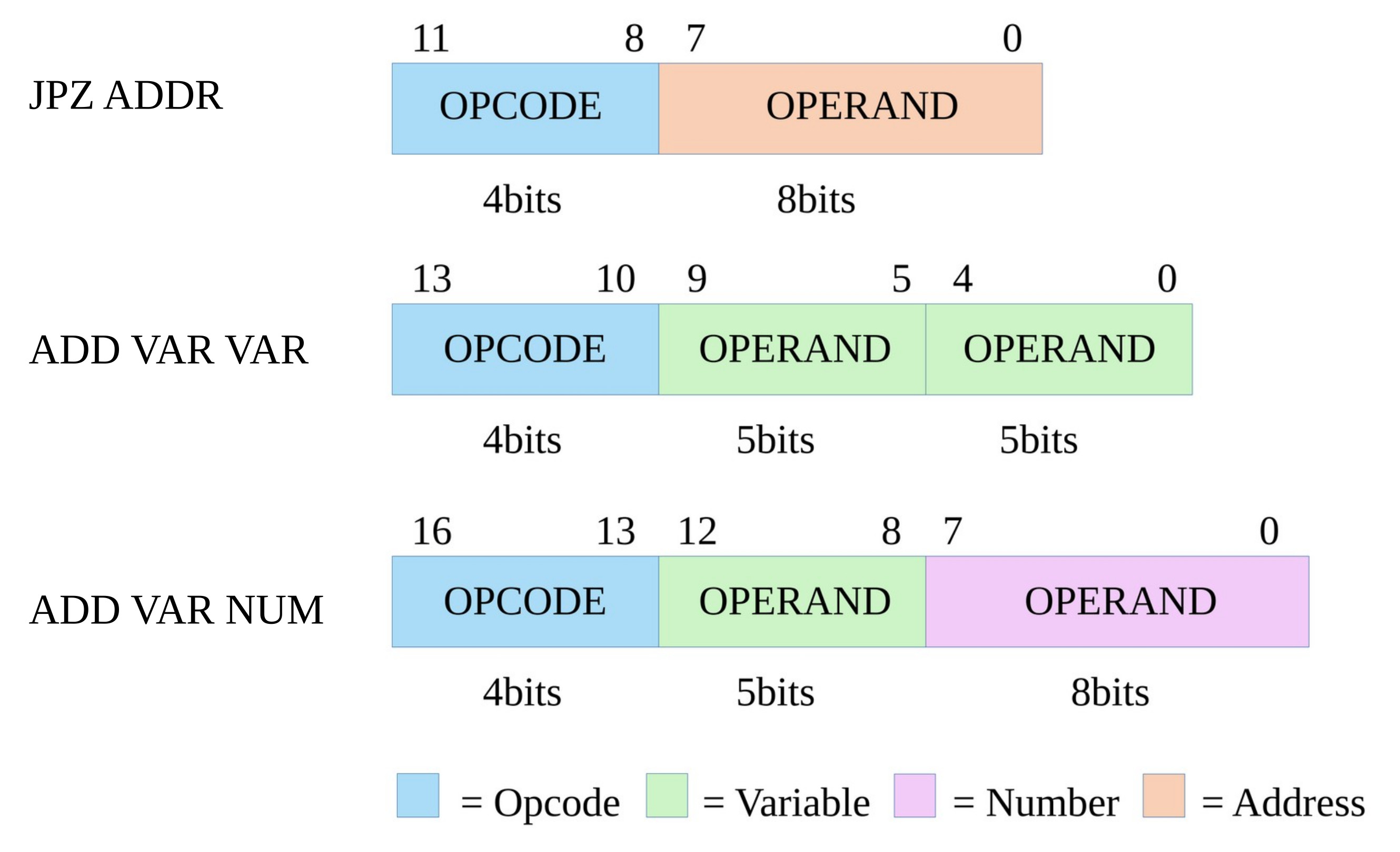
Figure 2 : initial instruction encoding
To reduce the instruction length to 16bits we need to loose a bit. To do this we could limit the NUMBER operand bit-field to 7bits, or limit the number of variables to 16 i.e. a 4bit VARIABLE operand bit-field, but that does have a big impact on the processor, limiting its data and instruction storage. Therefore, plan-B, reduce the opcode field to 3bits, and take advantage of the fact that the JPZ only has 1 operand, consider the following:
VARIABLE CODES
A = 00001        N = 01110
B = 00010        O = 01111
C = 00011        P = 10000
D = 00100        Q = 10001
E = 00101        R = 10010
F = 00110        S = 10011
G = 00111        T = 10100
H = 01000        U = 10101
I = 01001        V = 10110
J = 01010        W = 10111
K = 01011        X = 11000
L = 01100        Y = 11001
M = 01101        Z = 11010

INSTR          OPCODE  OPERAND0   OPERAND1
JPZ ADDR     : 000     00000      XXXXXXXX
ADD VAR VAR  : 000     XXXXX      XXXXX000
ADD VAR NUM  : 001     XXXXX      XXXXXXXX
AND VAR VAR  : 010     XXXXX      XXXXX000
AND VAR NUM  : 011     XXXXX      XXXXXXXX
XOR VAR VAR  : 100     XXXXX      XXXXX000
XOR VAR NUM  : 101     XXXXX      XXXXXXXX
OR  VAR VAR  : 110     XXXXX      XXXXX000
OR  VAR NUM  : 111     XXXXX      XXXXXXXX

INSTR FORMAT 0 : JPZ

OPCODE  NU     ADDR
FED     CBA98  76543210
000     00000  XXXXXXXX

INSTR FORMAT 1 : ADD VAR VAR

OPCODE  OPERAND0  OPERAND1   NU
FED     CBA98     76543      210
XXX     XXXXX     XXXXX      000

INSTR FORMAT 2 : ADD VAR NUM

OPCODE  OPERAND0  IMM
FED     CBA98     76543210
XXX     XXXXX     XXXXXXXX
There are three types of instructions, representing the three addressing modes used. All instructions are now a fixed length, 16bits in size, one instruction is stored in each memory location. The VARIABLE operand bit-field is now encoded using the values 1 to 26, rather than 0 to 25. The JPZ instruction is redefined to be not just the OPCODE field value, but also the value of OPERAND0 i.e. bits 12 to 8. Therefore, OPCODE=000 AND OPERAND0=00000 must both be true for the JPZ instruction to be executed. This allows OPCODE=000 to be reused for the ADD VAR VAR instruction, as its OPERAND0 bit-field will be a none zero value i.e. will be the value 1 to 26. Sooo, Type 0 instructions are JUMP instructions i.e. their operand is an ADDRESS. Type 1 instructions i.e. ADD VAR VAR, only need 13bits, therefore the lower 3bits are padded with zeros to increase their size to 16bits. Type 2 instructions are ADD VAR NUM instructions and use all 16bits, as shown in figure 3.
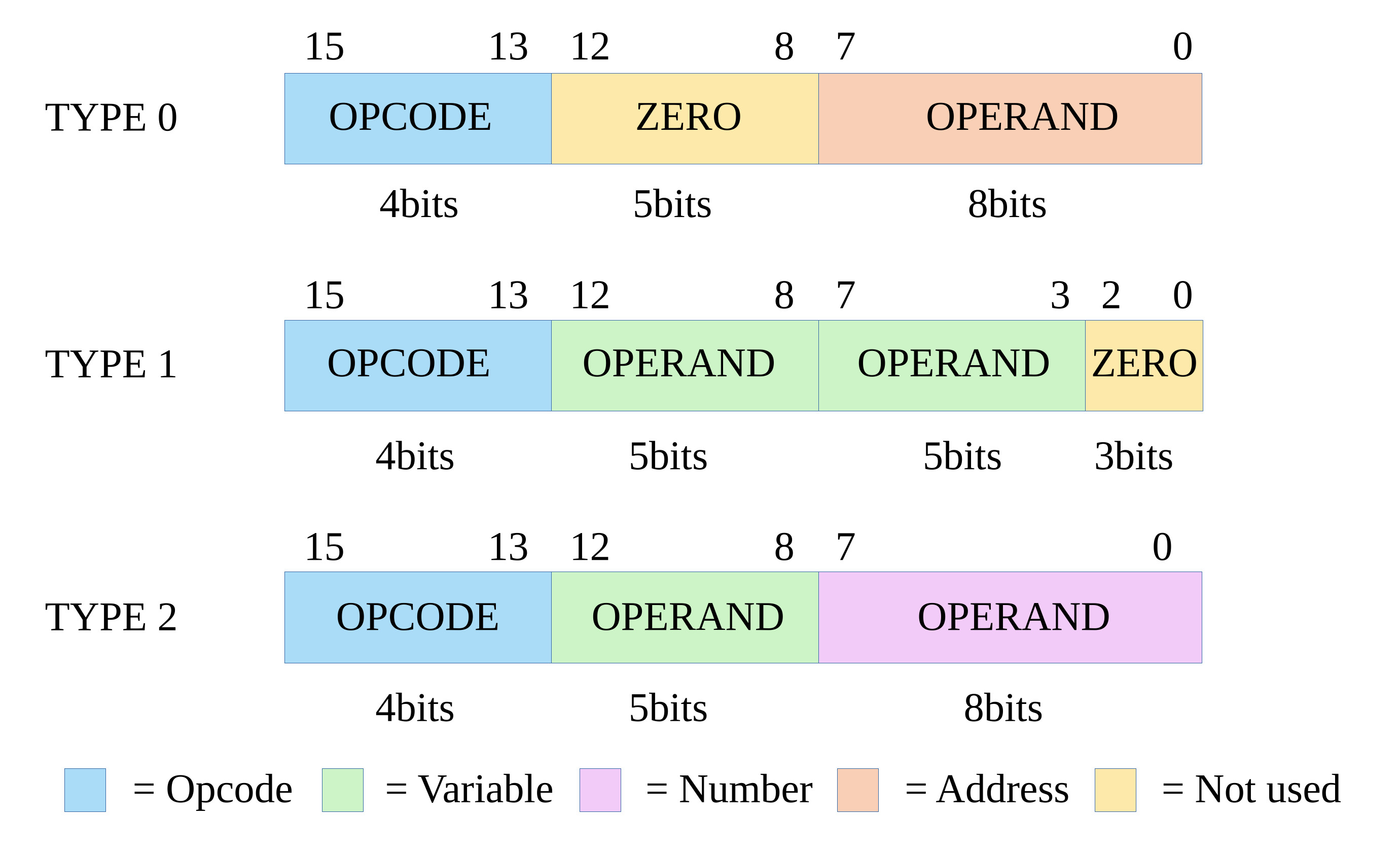
Figure 3 : final instruction encoding
Now we know what bit-fields are used in each instruction, sooo, the next step is to write an assembler, writing binary instruction by hand is tooo much fun i.e. raw machine code. This assembler is a cut-down version of the simpleCPUs assembler (Link), (Link), written in python, it converts minimalCPU assembly language programs into the raw binary machine code used by the processor. You can download a copy here: (minimalCPU_as.py).
#!/usr/bin/python
import getopt
import sys
import re

#############
# FUNCTIONS #
#############

def convertData(data):
  try:
    if '0x' in data:
      return int(data,16)
    elif '0b' in data:
      return int(data, 2)
    else:
      return int(data)
  except:
    print("Error: invalid operand can not convert")
    print(data)
    sys.exit(1)

################
# MAIN PROGRAM #
################

def minimalCPU_as(argv):

  if len(sys.argv) <= 1:
    print ("Usage: minimalCPU_as.py -i ")
    print ("                        -o ")
    return

  # init variables #
  version = '3.0'

  tmp_filename = 'tmp.asm'
  source_filename = 'default.asm'
  data_filename = 'default.dat'
  ram_filename = 'default.ram'
  mon_filename = 'default.mon'

  address = 0

  s_config = 'i:o:'
  l_config = ['input', 'output']

  input_file_present = False

  instruction_address = 0
  label_dictionary = {}
  instr_names = ['add', 'and', 'xor', 'or', 'jpz']

  # capture commandline options #
  try:
    options, remainder = getopt.getopt(sys.argv[1:], s_config, l_config)
  except getopt.GetoptError as m:
    print("Error: ", m)
    sys.exit(1)

  # extract options #
  for opt, arg in options:
    if opt in ('-o', '--output'):
      data_filename = arg + ".dat"
      ram_filename = arg + ".ram"
      mon_filename = arg + ".mon"
    elif opt in ('-i', '--input'):
      input_file_present = True
      if ".asm" in arg:
        source_filename = arg
      else:
        source_filename = arg + ".asm"

  # exit if no input file present #
  if input_file_present:

    # open files #
    try:
      print("Opening: " + source_filename )
      source_file = open(source_filename, "r")
    except IOError:
      print("Error: Input file does not exist.")
      sys.exit(1)

    try:
      tmp_file = open(tmp_filename, "w")
      data_file = open(data_filename, "w")
      ram_file = open(ram_filename, "w")
      mon_file = open(mon_filename, "w")
    except IOError:
      print("Error: Could not open output files")
      sys.exit(1)

    # scan through code, count instruction, check opcodes
    # and identify labels and assign addresses.

    instruction_address = address

    while True:
      line = source_file.readline()
      line = re.sub(r'#', '# ', line.lower())
      line = re.sub(r'\s+', ' ', line)

      if line == '':
        break

      if len(line) > 1 and line[0] == ' ':
        line = line[1:]

      if line[0] =='#' or line[0] ==' ':
        continue

      if ":" in line:
        key = re.sub(r':.$', '', line)
        if key in label_dictionary:
          print("Error: duplicate labels")
          print(key)
          sys.exit(1)
        else:
          label_dictionary[key] = instruction_address
      else:
        words = line.split(' ')
        if words[0] in instr_names:
          instruction_address += 1
        else:
          print("Error: invalid instruction -")
          print(words)
          sys.exit(1)

    # replace lables with addresses, write code to tmp_file

    source_file.seek(0)
    instruction_address = address

    while True:
      line = source_file.readline()
      line = re.sub(r'#', '# ', line.lower())
      line = re.sub(r'\s+', ' ', line)

      if line == '':
        break

      if len(line) > 1 and line[0] == ' ':
        line = line[1:]

      if line[0] =='#' or line[0] ==' ':
        continue

      if ":" in line:
        if "#" in line:
          print("Error: can not have comments on the same line as labels")
          print(line)
          sys.exit(1)
        else:
          continue

      words = line.split(' ')
      outputString = str.format('{:03}', instruction_address) + " "

      for i in range(0, len(words)):
        if words[i] in label_dictionary:
          key = words[i]
          outputString = outputString + " " + str(label_dictionary[key])
        else:
          if words[i] != '':
            outputString = outputString + " " + words[i]

      outputString = outputString + "\n"
      tmp_file.write( outputString )
      instruction_address += 1

    source_file.close()
    tmp_file.close()

    # open TMP file #

    try:
      tmp_file = open(tmp_filename, "r")
    except IOError:
      print("Error: could not output temp file")
      sys.exit(1)

    # vhdl ram text

    ram_file.write( "  signal ram : ram_type := (\n" )

    # generate machine code

    while True:
      line = tmp_file.readline()
      line = re.sub(r'\s+', ' ', line)

      if line == '':
        break

      words = line.split(' ')
      instr = 0

      # match opcode

      if words[0].isdigit():
        # ADD X Y, ADD X 1
        if words[1] == "add":
          if words[2].isalpha() and words[3].isalpha():
            instr = int('0000000000000000', 2)
            instr = instr | ((ord(words[2]) - 96) << 8)
            instr = instr | ((ord(words[3]) - 96) << 3)
          elif words[2].isalpha() and words[3].isdigit():
            instr = int('0010000000000000', 2)
            instr = instr | ((ord(words[2]) - 96) << 8)
            instr = instr | (int(words[3]) & 0xFF)
          else:
            print("Error: invalid operand")
            print(words)
            sys.exit(1)

        # AND X Y, AND X 1
        elif words[1] == "and":
          if words[2].isalpha() and words[3].isalpha():
            instr = int('0100000000000000', 2)
            instr = instr | ((ord(words[2]) - 96) << 8)
            instr = instr | ((ord(words[3]) - 96) << 3)
          elif words[2].isalpha() and words[3].isdigit():
            instr = int('0110000000000000', 2)
            instr = instr | ((ord(words[2]) - 96) << 8)
            instr = instr | (int(words[3]) & 0xFF)
          else:
            print("Error: invalid operand")
            print(words)
            sys.exit(1)

        # XOR X Y, XOR X 1
        elif words[1] == "xor":
          if words[2].isalpha() and words[3].isalpha():
            instr = int('1000000000000000', 2)
            instr = instr | ((ord(words[2]) - 96) << 8)
            instr = instr | ((ord(words[3]) - 96) << 3)
          elif words[2].isalpha() and words[3].isdigit():
            instr = int('1010000000000000', 2)
            instr = instr | ((ord(words[2]) - 96) << 8)
            instr = instr | (int(words[3]) & 0xFF)
          else:
            print("Error: invalid operand")
            print(words)
            sys.exit(1)

        # OR X Y, OR X 1
        elif words[1] == "or":
          if words[2].isalpha() and words[3].isalpha():
            instr = int('1100000000000000', 2)
            instr = instr | ((ord(words[2]) - 96) << 8)
            instr = instr | ((ord(words[3]) - 96) << 3)
          elif words[2].isalpha() and words[3].isdigit():
            instr = int('1110000000000000', 2)
            instr = instr | ((ord(words[2]) - 96) << 8)
            instr = instr | (int(words[3]) & 0xFF)
          else:
            print("Error: invalid operand")
            print(words)
            sys.exit(1)

        # JPZ
        elif words[1] == "jpz":
          if words[2].isdigit():
            instr = int('0000000000000000', 2)
            instr = instr | (int(words[2]) & 0xFF)
          else:
            print("Error: invalid operand")
            print(words)
            sys.exit(1)
        else:
          print("Error: invalid opcode")
          print(words)
          sys.exit(1)

        print( str.format('{:016b}', instr) )

        instruction_address = int(words[0])
        data_file.write(str.format('{:04}', instruction_address) + ' ')
        bin_value = str.format('{:016b}', instr)
        data_file.write( bin_value )
        data_file.write("\n")

        ram_file.write(f'    {instruction_address:<6d} => "{bin_value}",\n')
        mon_file.write(f"{instruction_address:04X}:{instr:04X}\n")

    # close files #
    tmp_file.close()
    data_file.close()
    mon_file.close()

    # finish vhdl ram text
    ram_file.write("    others => (others => '0')\n")
    ram_file.write("  );\n")
    ram_file.close()

    print("closed")

  else:
    print("Error: Input file not specified")
    sys.exit(1)

if __name__ == '__main__':
  minimalCPU_as(sys.argv)
To run this assembler refer to the tutorials / information on this webpage: (Link), however, the condensed version is open a command prompt, CD into the folder containing the minimalCPU_as.py and assembly language file, then execute the command shown in figure 4. You can download a copy of the test code here: (test.asm).
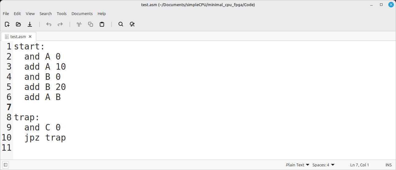
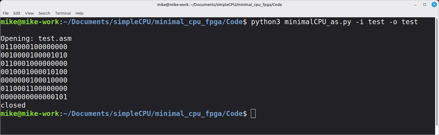
Figure 4 : assembly code (top), assembler (bottom)
Note, in this example the assembly program is the file test.asm, a simple program that initialises variables A=10 and B=20, then adds these values A=A+B=30. Key thing to remember is that the assembler and the source file must be in the same directory, alternatively you can specify the absolute / relative path using the -i parameter.
If all is good and you have no syntax errors the assembler will produce 3 output files as shown in figure 5. These all say the same thing but in different formats i.e. each specifies an address in memory and its data. In the .dat file the first column is a decimal address, the second is binary data i.e. an instruction. The .ram is a VHDL array declaration that can be used to initialise memory in the FPGA, defining the index and its data. Finally, there is the .mon file, this defines the address:data, both values are in hexadecimal i.e. base 16. This file can be uploaded into the FPGA using the monitor component (discussed later). You can download a copy of these files here: (test.dat), (test.ram) and (test.mon).
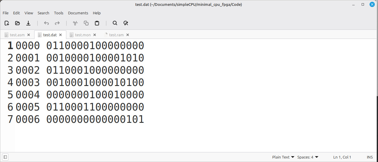
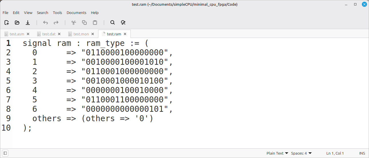
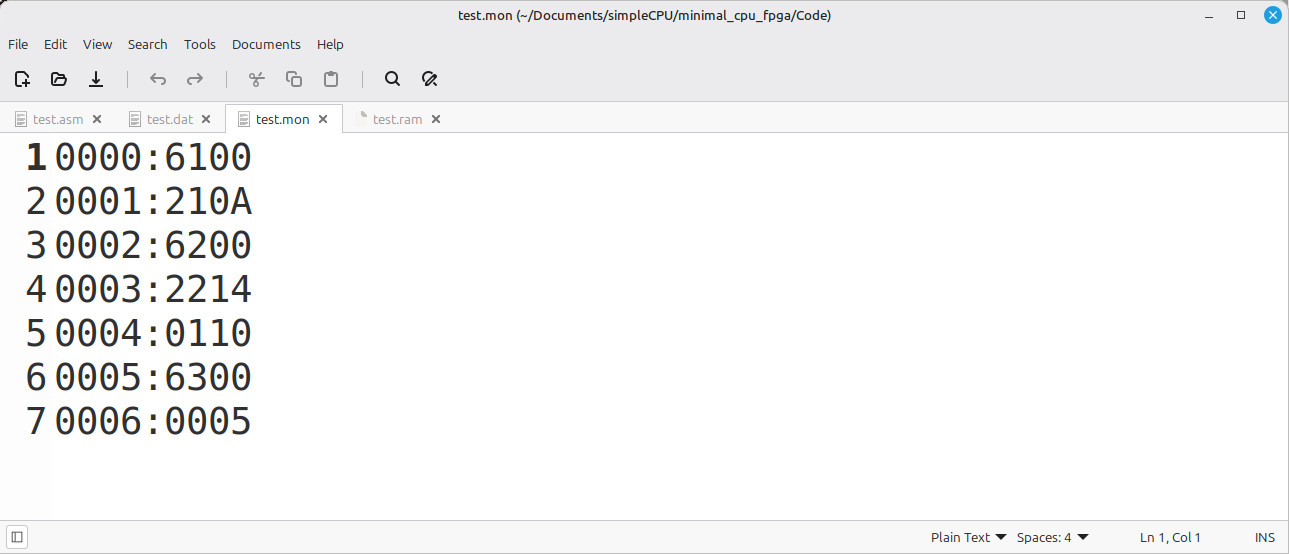
Figure 5 : output files, dat (top), ram (middle) and mon (bottom)
The complete minimalCPU FPGA system is shown in figure 6. The minimalCPU component is connected to code_memory which stores its program / instructions, and variable_memory which stores its data i.e. variables A - Z. In addition to these core components, there are components that generate the clocks and reset signals and allow programs to be uploaded and downloaded using a serial terminal. These are discussed below, but at this stage these components can be considered "black boxes", components we will look at these in more detail at a later time.
Note, to save time, except for the top-level schematics all components where implemented in VHDL (Link)
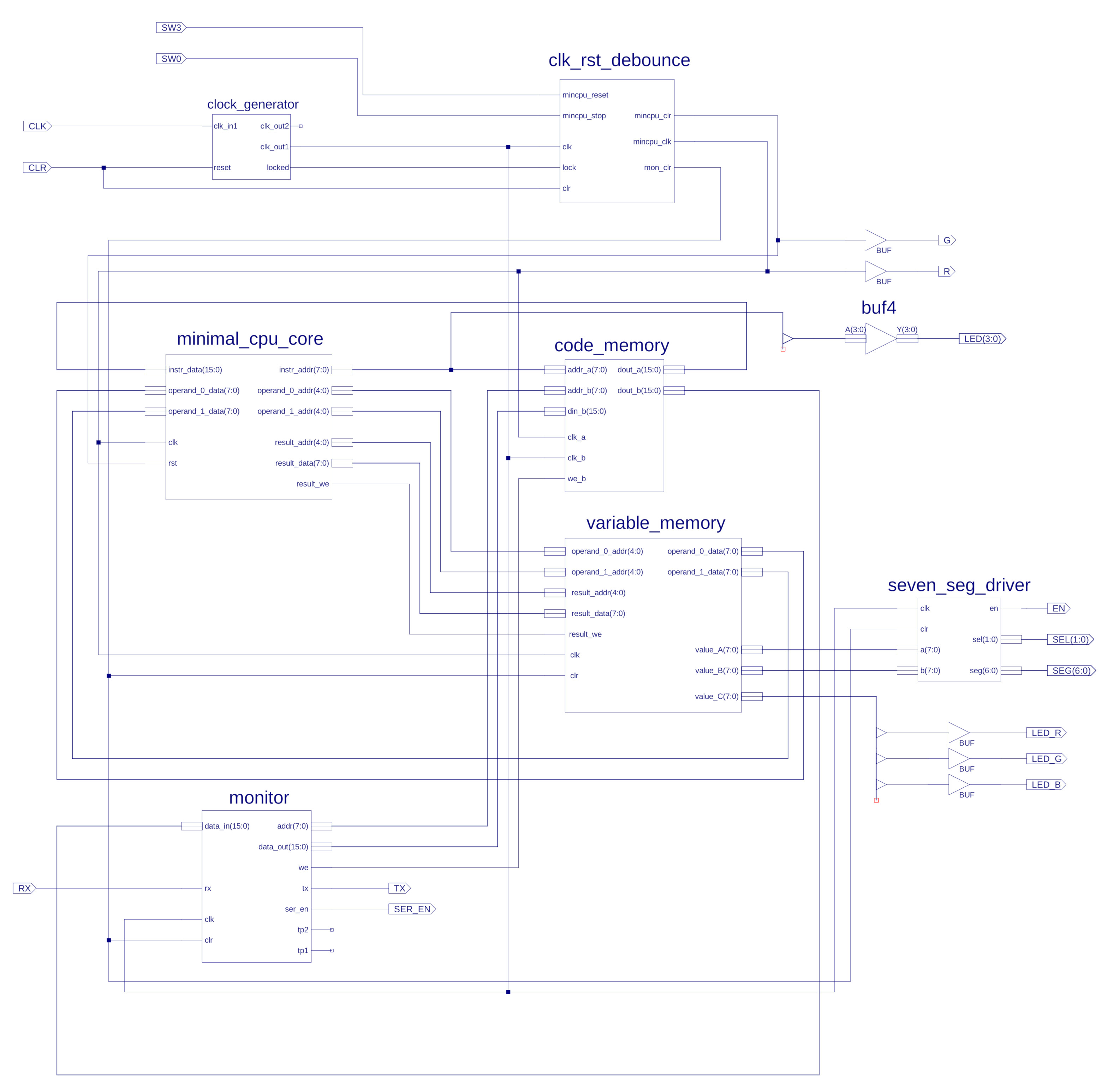
Figure 6 : top level schematic
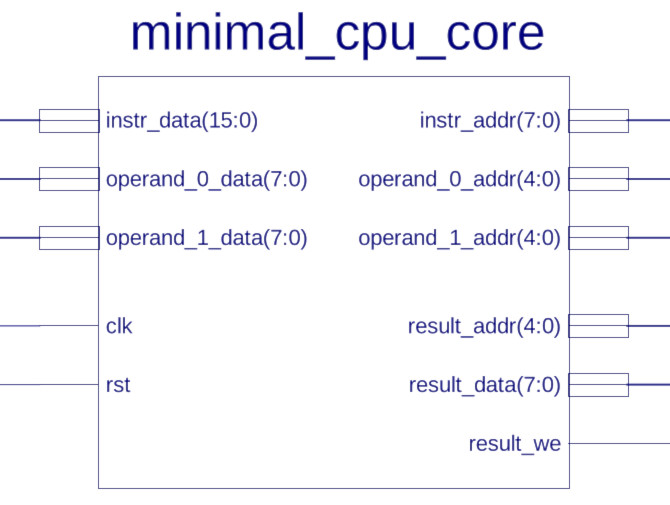
Figure 7 : minimalCPU component
A component has inputs and outputs, typically inputs are on the left, outputs are on the right. To communication with its memory components the minimalCPU uses its address, data and control buses (Link). This component has the following input/output ports:
A bus is just a collection of wires used to transfer a binary value e.g. the instr_data bus transfers instructions, instructions (figure 3) are 16bits long, so we need 16 wires to transfer that value. Address buses specify what memory location to access. Data buses are used to transfer data to/from this location and the processor. Control bus define the operations to be performed on a bus e.g. result_we, when set high (1) it tells memory that the value on the result_data bus is valid and can be written to memory, if set low (0) data is not valid.
The internals of the minimalCPU are implemented in VHDL (Link), i don't want confuse people here by explaining how this hardware works, sooo, we will only consider the operation of this processor in terms of its state-machine, its pseudo code description shown below:
SWITCH STATE:
  CASE RESET:
    PROGRAM_COUNTER = 0
    ZERO_FLAG = 0
    RESULT_WE = 0
    STATE = GET_INSTRUCTION

  CASE GET_INSTRUCTION:
    RESULT_WE = 0
    INSTR_ADDR = PROGRAM_COUNTER
    STATE = EXECUTE_INSTRUCTION

  CASE EXECUTE_INSTRUCTION:
    IF INSTR_DATA(15:13) = 000 AND INSTR_DATA(12:8) = 00000000
    THEN
      RESULT_WE = 0
      IF ZERO_FLAG = 1
      THEN
        PROGRAM_COUNTER = INSTR_DATA(7:0)
      ELSE
        PROGRAM_COUNTER = PROGRAM_COUNTER + 1
      END IF
      STATE = GET_INSTRUCTION

    ELSE
      SWITCH INSTR_DATA(15:13):
        CASE 000:
          RESULT_DATA = OPERAND_0_DATA + OPERAND_1_DATA
        CASE 001:
          RESULT_DATA = OPERAND_0_DATA + INSTR_DATA(7:0)
        CASE 010:
          RESULT_DATA = OPERAND_0_DATA & OPERAND_1_DATA
        CASE 011:
          RESULT_DATA = OPERAND_0_DATA & INSTR_DATA(7:0)
        CASE 100:
          RESULT_DATA = OPERAND_0_DATA ^ OPERAND_1_DATA
        CASE 101:
          RESULT_DATA = OPERAND_0_DATA ^ INSTR_DATA(7:0)
        CASE 110:
          RESULT_DATA = OPERAND_0_DATA | OPERAND_1_DATA
        CASE 111:
          RESULT_DATA = OPERAND_0_DATA | INSTR_DATA(7:0)
        DEFAULT:
          RESULT_DATA = 0
      END SWITCH

      IF RESULT_DATA = 0
      THEN
        ZERO_FLAG = 1
      ELSE
        ZERO_FLAG = 0
      END IF

      RESULT_WE = 1
      PROGRAM_COUNTER = PROGRAM_COUNTER + 1
      STATE = GET_INSTRUCTION
    END IF

  DEFAULT:
    STATE = RESET
END SWITCH
The processor's internal functions are controlled by three variables:
On power-up hardware within the clk_rst_debounce component pulses the processor's reset pin. The processor then alternates between the GET_INSTRUCTION and EXECUTE_INSTRUCTION phases, reading an instruction, decoding its OPCODE and processing its OPERANDS. These state transitions are triggered by the system clock, a square wave signal that repeatedly switches between a logic 1 and 0, as shown in figure 8. On each rising clock edge the state-machine switches between the GET_INSTRUCTION and EXECUTE_INSTRUCTION states i.e. an instruction takes two clock cycles to complete, two clock periods worth of time.
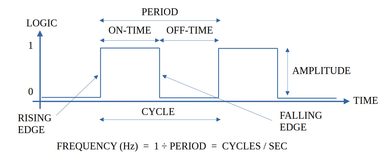
Figure 8 : system Clock
Note, to see how these internal operations are implemented in more detail have a look at the simpleCPU processors on the main webpage.
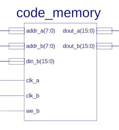
Figure 9 : Code memory component
This is the memory used to store the minimalCPU's program, each memory location contains one 16bit instruction, address range: 0 to 255. This memory differs from your typical memory having two interfaces i.e. two address buses. This dual port memory allows two different components to access this memory at the same time i.e. the minimalCPU and the monitor component. The minimalCPU component is connected to port A, allowing it to read instructions from memory. The monitor component is connected to port B, allowing it to read and write values to memory i.e. to access memory at the same time as the minimalCPU. This second interface allows the user to upload and download programs to/from code_memory (described later). This component has the following input/output ports:
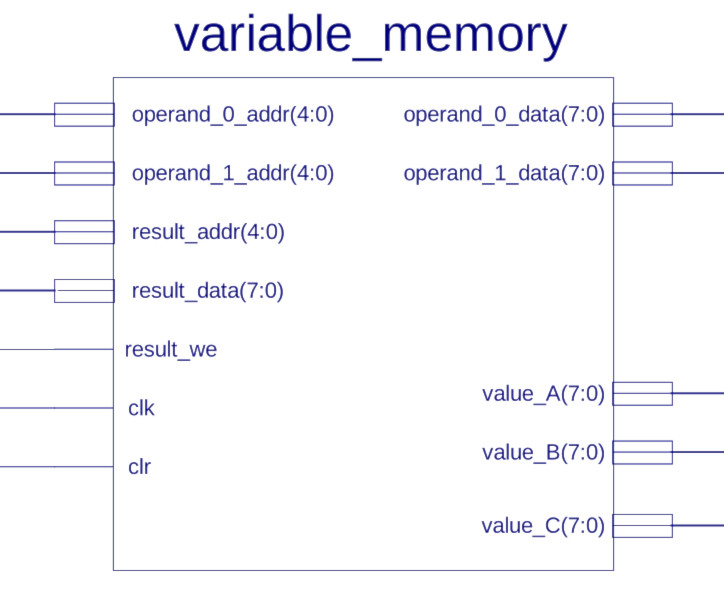
Figure 10 : Variable memory component
This memory is used to store data variables A to Z, each variable can store an 8bit value i.e. the number 0 to 255. Again, another example of multi-port memory. This memory has two read ports and one write port. These are required to support instruction like: ADD VAR VAR i.e. instructions that read two variables and write back the result to the same memory. This component has the following input/output ports:
Note, three additional output ports have been added to this memory component: value_A, value_B and value_C, output the variable values contained in variables A, B and C. These are debug output buses, allowing the user to monitor variables A and B on the seven segment display. Variable C bits C(2:0) are connects to the RGB LED i.e. RED=C(0), GREEN=C(1), BLUE=C(2), C(7:3) are not connected, sooo, storing the value 1 to C will turn the LED red.
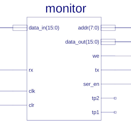
Figure 11 : Monitor component
Serial monitor component, allows test programs to be uploaded into the minimalCPU's code_memory, can also be used to read instructions in code_memory, download programs so that they can be saved to a files for later use. At the heart of this component is a simpleCPUv1d2 running the serial monitor program MikeMon, for more information refer to this webpage:(Link). This component has the following input/output ports:
Note, instructions on how to use this component are discussed later.
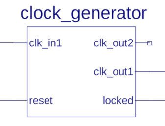
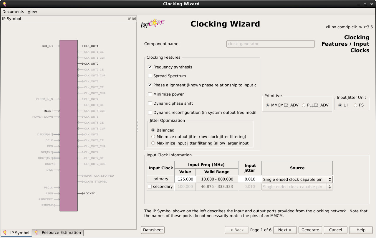
Figure 12 : Clock generator component
The systems clock signal is generated from the FPGA board's clock oscillator. This has a frequency of 125MHz i.e. a square wave, producing 125,000,000 clock cycles per second. To reduce this frequency down to the 25MHz used by the monitor component the Xilinx clock wizard IP-core generator is used, as shown in figure 12. This component has the following input/output ports:
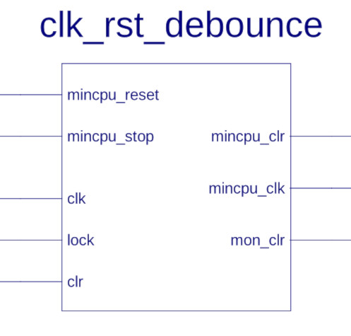
Figure 13 : Clock Reset Debounce component
This component is a container component i.e. simplifies, removed clutter from top-level schematic. Its internal schematic is shown in figure 14.
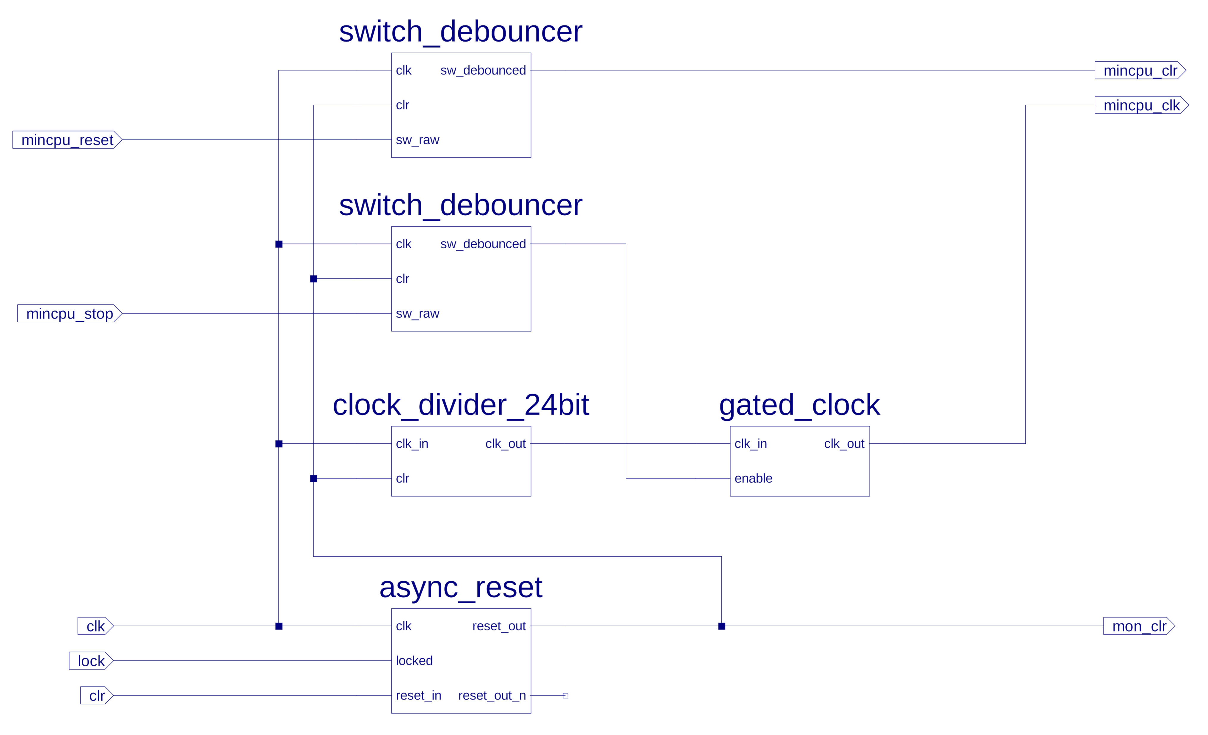
Figure 14 : Clock Reset Debounce schematic
Note, for more information on switch debounce refer to here: (Link).
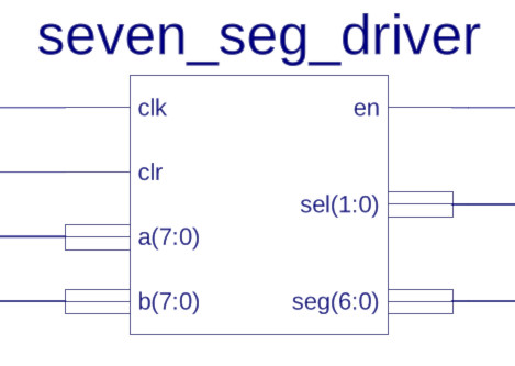
Figure 15 : Seven Segment Decoder component
To allow the user to see what is happening inside the FPGA we need to connect some of the internal signals and buses to LEDs. The seven_seg_decoder displays two 8bit values on a 4 digit seven segment hexadecimal display i.e. each 8bit value is displayed as two 4bit hex nibbles, each nibble is displayed on a seven segment display. This component has the following input/output ports:
To save hardware the four seven-segment displays share the same data bus: seg i.e. they are multiplexed (Link), as shown in figure 16. To updated these displays a digit is selected using the sel bus, the 4bit nibble is decoded using the truth table shown in figure 17 and written to the seg data bus, the enable line (en) is pulsed low. The sel bus is updated to select the next digit and the process repeats. This simple state-machine is implemented in hardware within this component, repeated reading the values on the a(7:0) and b(7:0) input buses, converting these to hexadecimal and writing these values to the seven segment display.
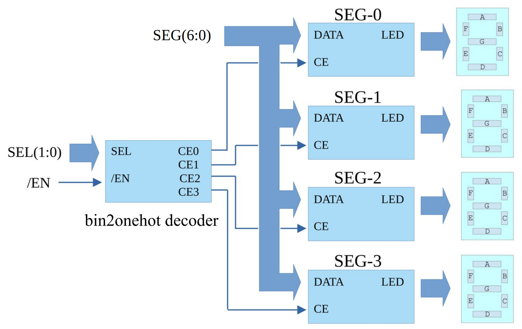
Figure 16 : Seven segment display hardware
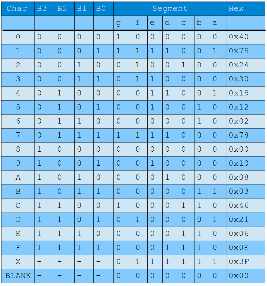
Figure 17 : binary nibble to seven segment truth table
The a(7:0) and b(7:0) buses are connected to the value_A and value_B buses from the variable_memory component, allowing the user to see the values in variables A and B, as shown in figured 18 and 19. The lower three bits of variable C are connected to the RGB LED shown in figure 20 i.e. RED=C(0), GREEN=C(1), BLUE=C(2), C(7:3) are not connected. Therefore, writing 1 to C will turn the LED red, writing 2 will set it green, 4 blue and 7 white etc.
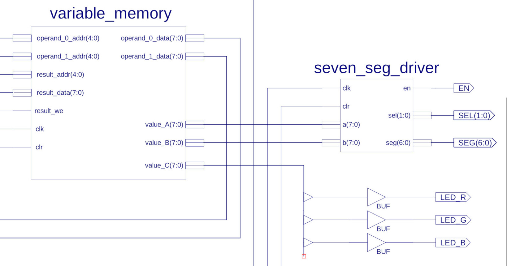
Figure 18 : Seven segment decoder in top-level schematic
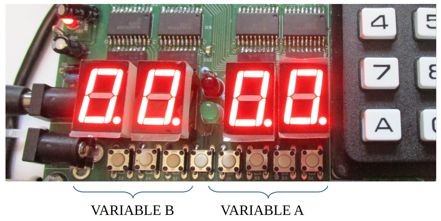
Figure 19 : Seven segment displays
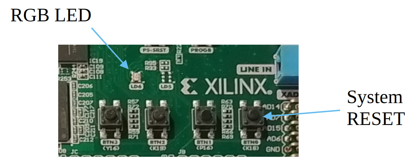
Figure 20 : RGB LED
To allow the user to see what instruction is currently being processed the lower four bits of the instr_addr bus are connected to four green LEDs. This address bus is driven by the minimalCPU's program_counter i.e. is the address of the current instruction being processed. The minimalCPU's clock and reset signals are connected to the 5mm RED and GREEN LEDs, as shown in figures 21 and 22.
Note, the instr_addr bus is an 8bit bus, so the user can not see all eight bits i.e. address 16 (00010000) and address 0 (00000000) will look the same, however, minimalCPU test programs tend to be on the small side, sooo most fit within the first 16 memory locations, but do remember that after address 15 the value displayed will roll over back to 0.
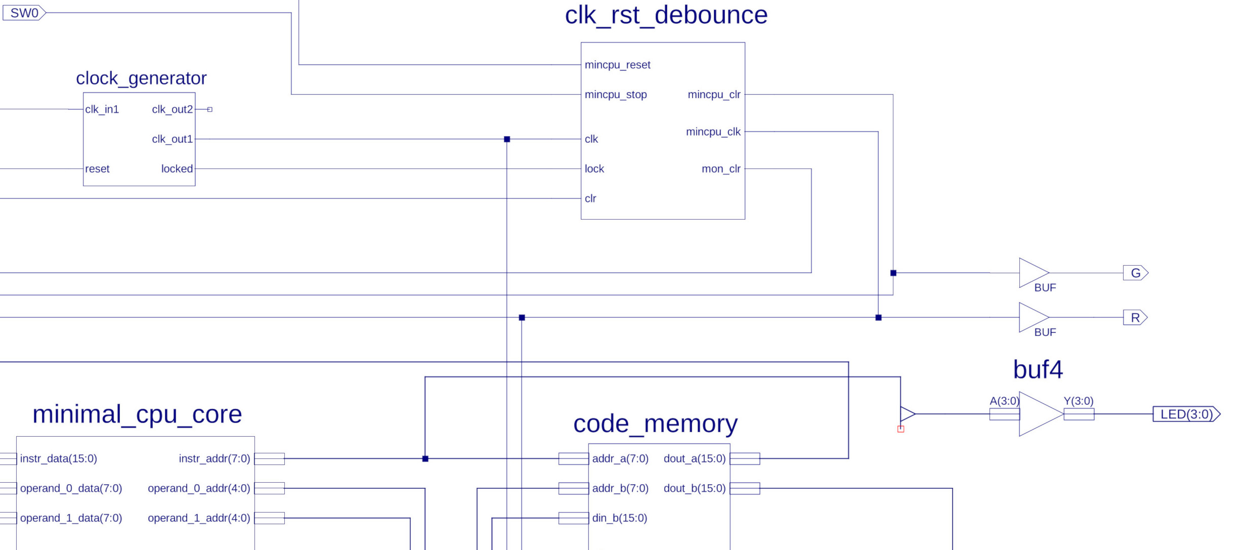
Figure 21 : code_memory address, clock and reset LEDs
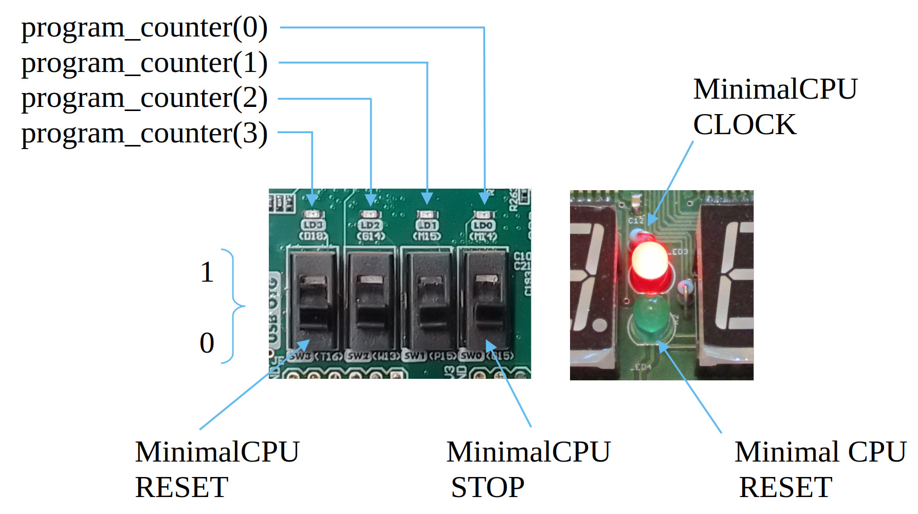
Figure 22 : Switches and LEDs
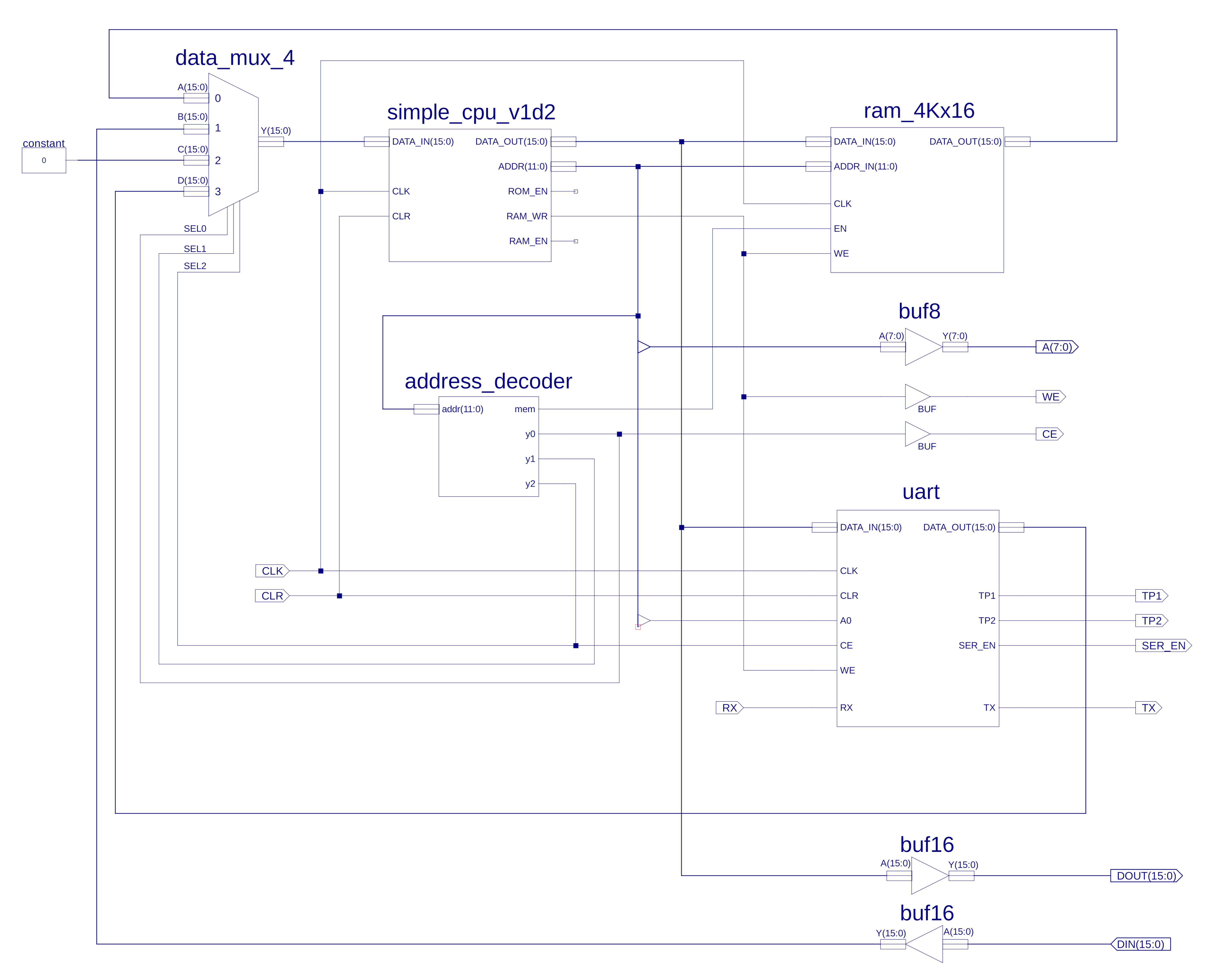
Figure 23 : monitor schematic
The monitor component's hardware is based on the simpleCPUv1d2 processor + UART i.e. serial port, as shown in figure 23. This hardware allows the user to read and write to the minimalCPU's code_memory via a serial terminal. The software running on the simpleCPUv1d2 is a modified version of the monitor program: MikeMon, described here: (Link). The simpleCPUv1d2 maps the minimalCPU's address space into its memory map: address 0xE00 to 0xEFF, as shown in figure 24.
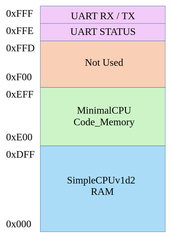
Figure 24 : memory map
The monitor program has been updated to only allow the user to read / write to this shared memory. The monitor code maps address range 0x00 - 0xFF, to 0xE00 - 0xEFF i.e. if the user requests to reads address range 0.FF, memory locations 0xE00 to 0xEFF will be read, as shown in figure 25.
Note, the machine code shown in this example is the previously described test program: test.asm.
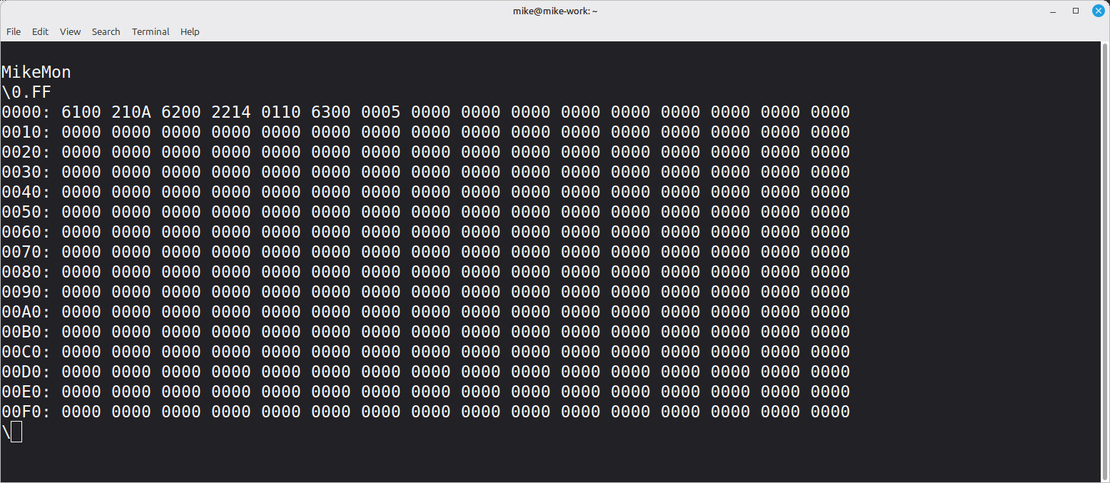
Figure 25 : reading memory
In addition to reading code_memory the user can also write data into this memory as shown in figure 26. In this example the instruction stored at address 1 i.e. ADD A 10, machine code: 0x210A, is replace with the instruction: ADD A 1, machine code 0x2101. When this program is executed the calculation A=1+20 will now be performed.
Note, whilst code_memory is being updated the minimalCPU can be reset AND stopped using the switches shown in figure 22. Then once memory has been updated, the minimalCPU can be restarted by moving these switches to the 0 position.
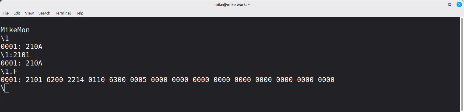
Figure 26 : writing memory
As discussed on the MikeMon webpage: (Link), the monitor program does have a flow-control issue i.e. it is possible to overflow the RX buffer if data is sent too quickly. Therefore, it is best to use the simple_cpu_terminal_v1.py terminal program as this adds the required char delays. You can download this python file here: (simple_cpu_terminal_v1.py). However, as the simpleCPUv1d2 RAM is not needed to store programs / data, the RX and TX buffers used have been increased to 1024 (0x3FF) characters, which is large enough for most minimalCPU programs, sooo, any terminal should be fine. Finally, the RUN function supported by the original MikeMon code has been disabled, as the simpleCPUv1d2 does not run the minimalCPU code.
Login to a lab PC, download the bit-file: (top_level.bit) and save to the folder "C:\User Files". Connect the FPGA to the PC as described in SYS1 lab1 and open the the Xilinx VM. Set the toggle switches on the FPGA board to the positions shown in figure 27 i.e. minimalcpu is RESET (5mm GREEN LED on) and STOPPED (5mm RED LED off).
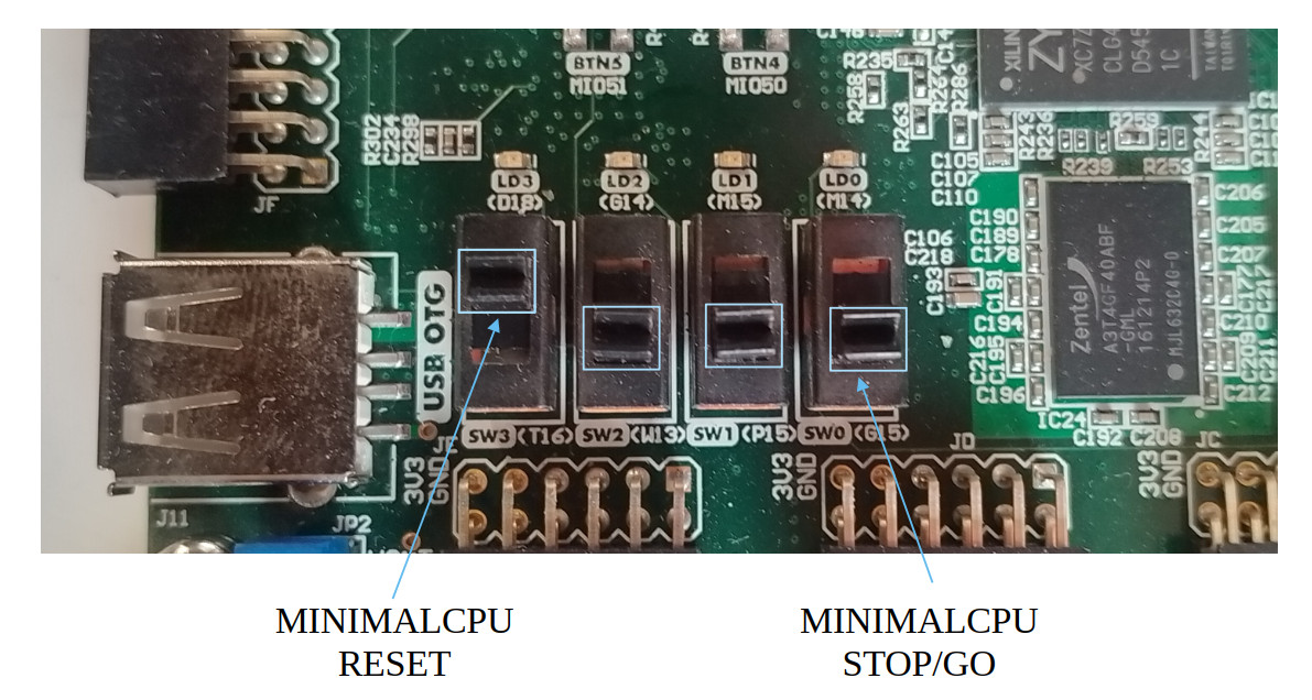
Figure 27 : MinimalCPU reset and stop switches
To configure the FPGA i.e. upload the top_level bit-file, follow the following steps:
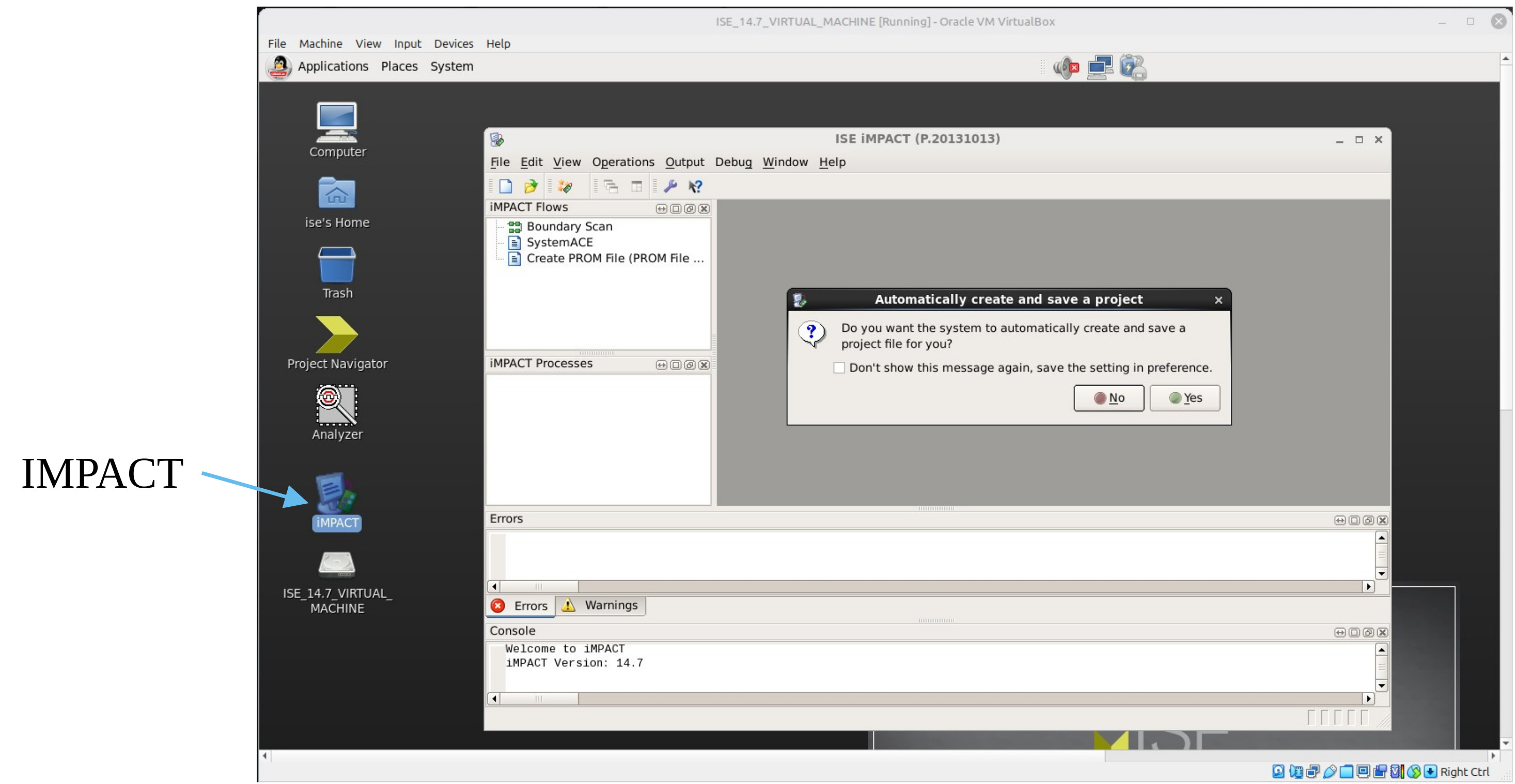
Figure 28 : Xilinx Virtual Machine
STEP 1: double left click on the iMPACT icon to launch the FPGA programming tool. You will be prompted to "Automatcally create and save a project" click on No, as shown in figure 28. The "New iMPACT Project" window will appear click Cancel. Basically click No or Cancel until pop-up windows stop appearing :).
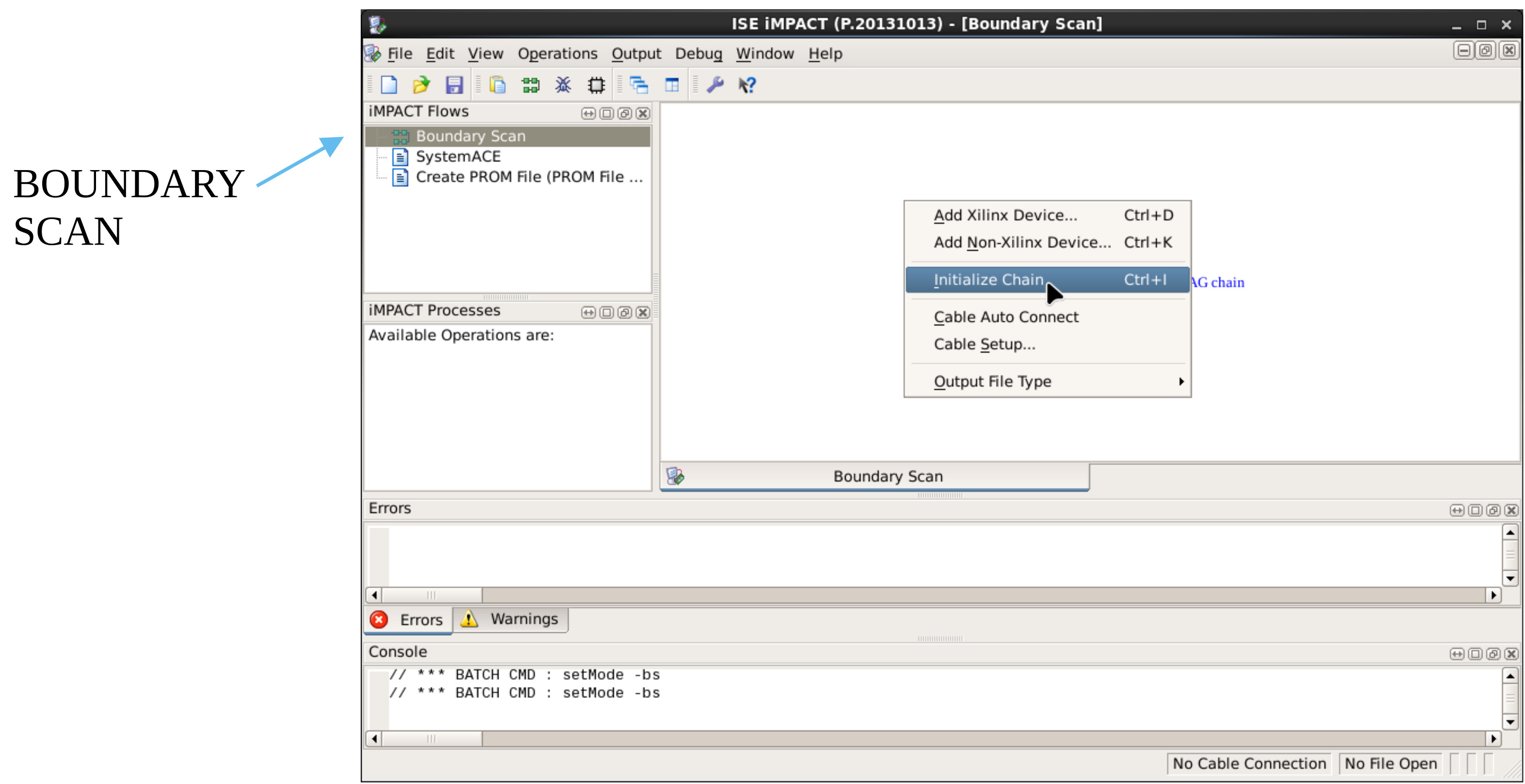
Figure 29 : Boundary scan
STEP 2: double left click on the "Boundary Scan" option, then right click anywhere in the main window and select "Initialise Chain", as shown in figure 29.
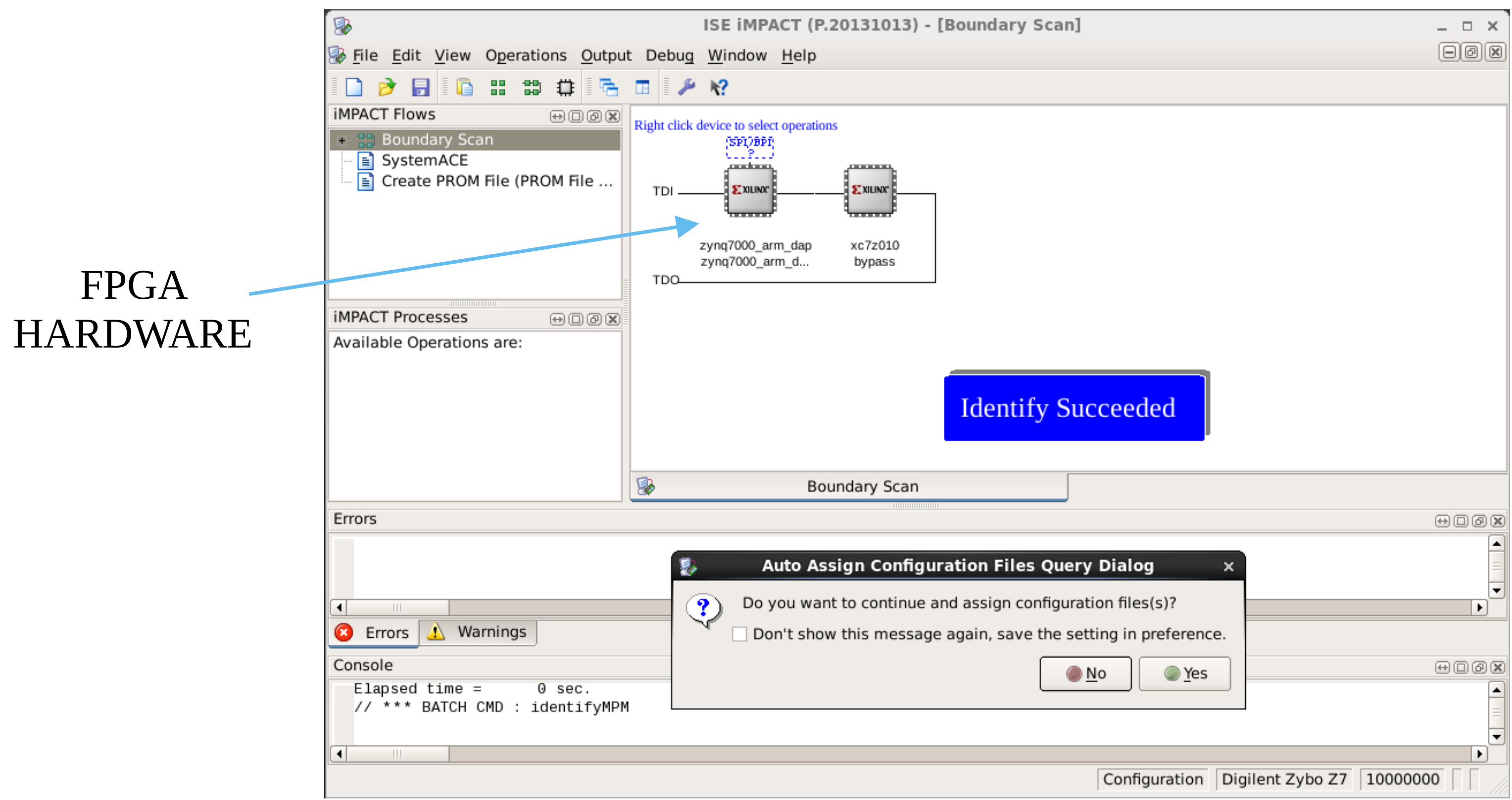
Figure 30 : Assign configuration files
STEP 3: if the FPGA board is correctly connected the FPGA hardware will be identified, as shown in figure 30. The "Auto Assign Configuration Files Query Dialog" window will then open, click Yes. If you do not see these two chip icons appear check that the FPGA board is connected and its power switch is in the ON position.
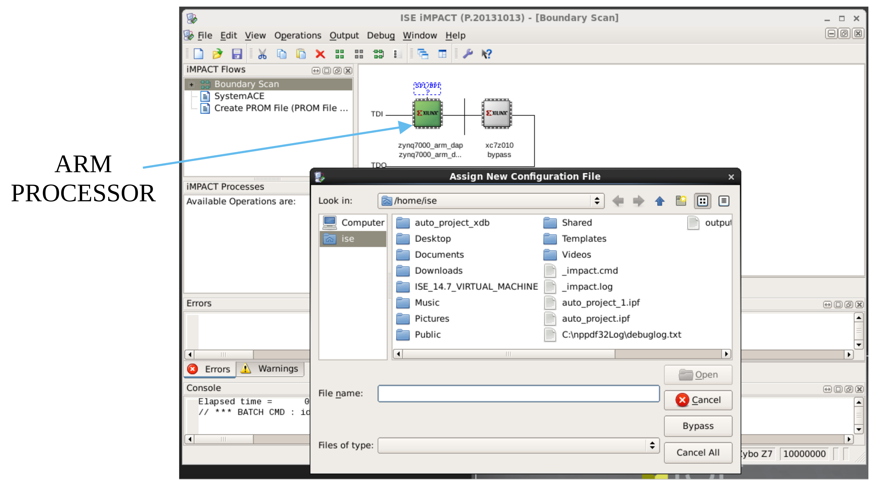
Figure 31 : Assign configuration file to ARM processor core
STEP 4: the ARM processor core icon will turn green allowing you to assign it a configuration files, as shown in figure 31. We are not using this hardware, so click Bypass.
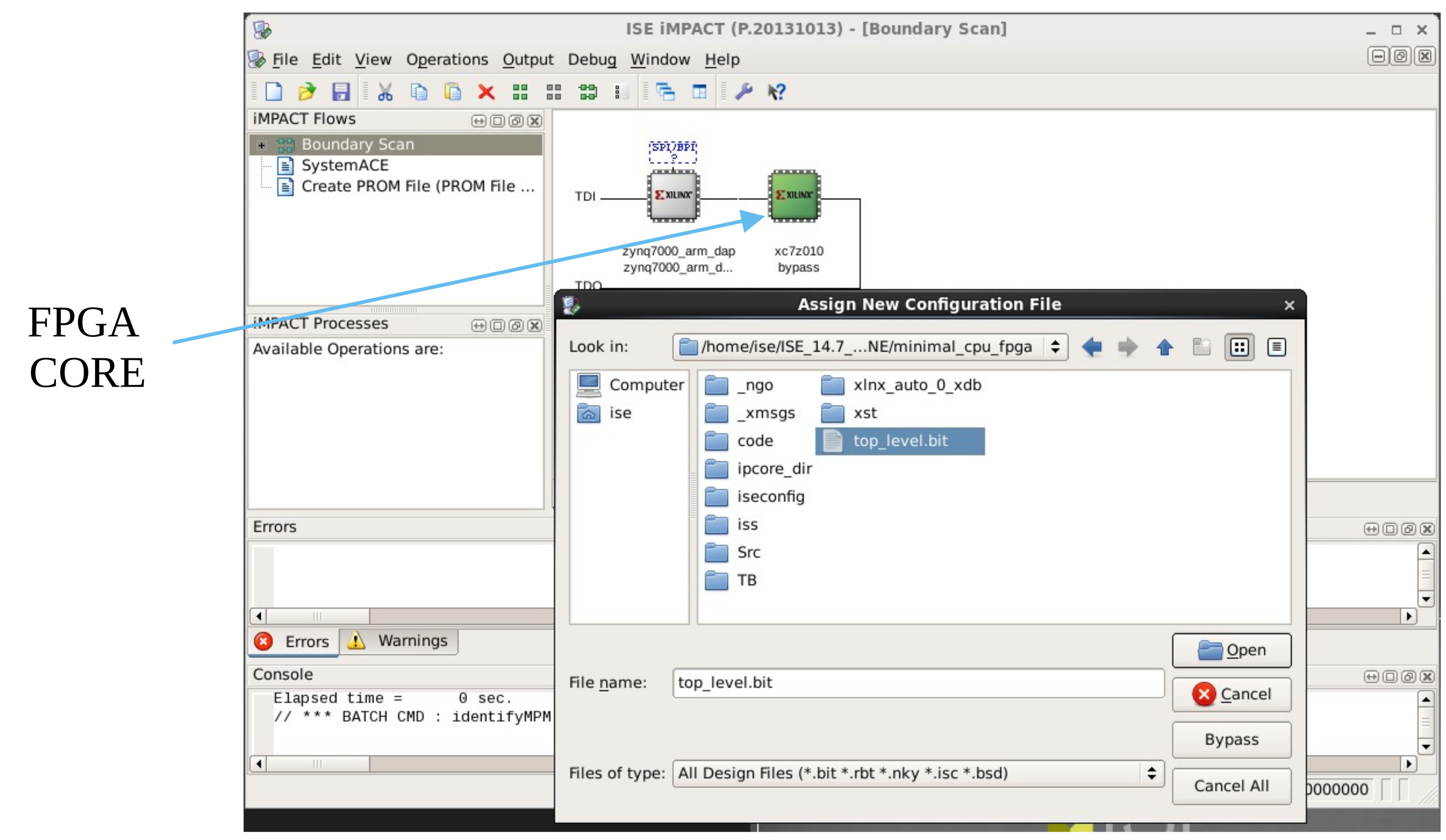
Figure 32 : Assign configuration file to FPGA core
STEP 5: the FPGA core icon will turn green allowing you to assign it a configuration files, as shown in figure 32. Browse to the Shared folder as described in SYS1 lab1 and select the top_level.bit file you previously downloaded, then click Open. The "Device Programming Properties" window will now open, click Ok. Note, the folders shown in figure 32 are on my laptop, your folder will differ.
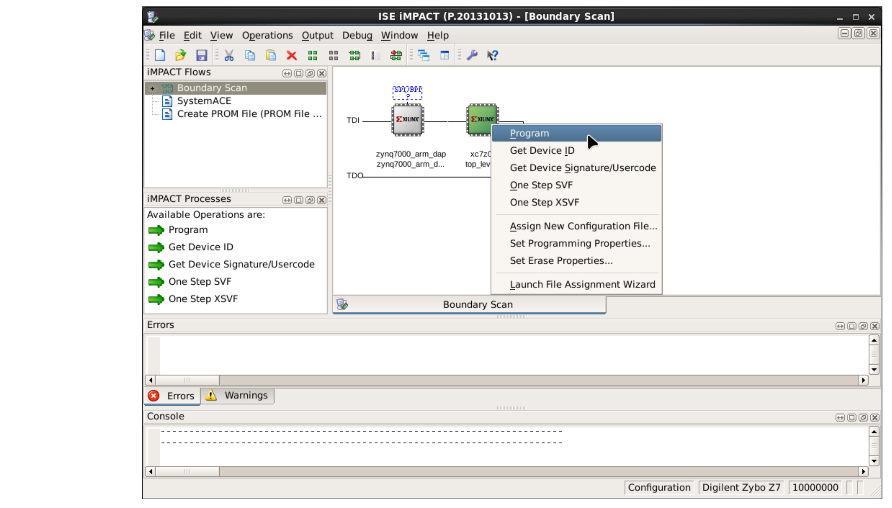
Figure 33 : Program FPGA core
STEP 6: right click on the FPGA core icon and select Program, as shown in figure 33. The "Device Programming Properties" window will now open, click Ok. A progress bar will appear showing the percentage of the top_level.bit file uploaded. When complete a blue Program Succeeded message will be displayed, as shown in figure 34.
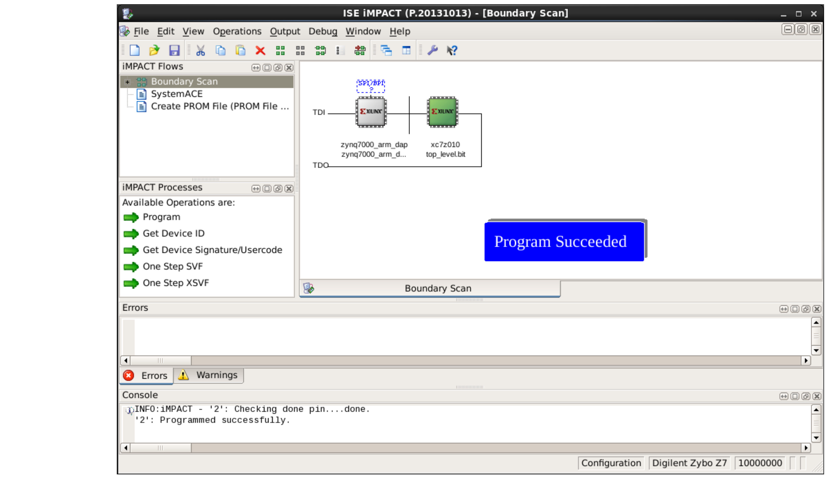
Figure 34 : FPGA core programmed successfully
The uploaded bit-file configures the minimalCPU's code_memory with the program shown in figure 35. This program sets the variables A=0, B=0 and C=1 i.e. sets the seven segment displays to 0 and the RGB LED to red.
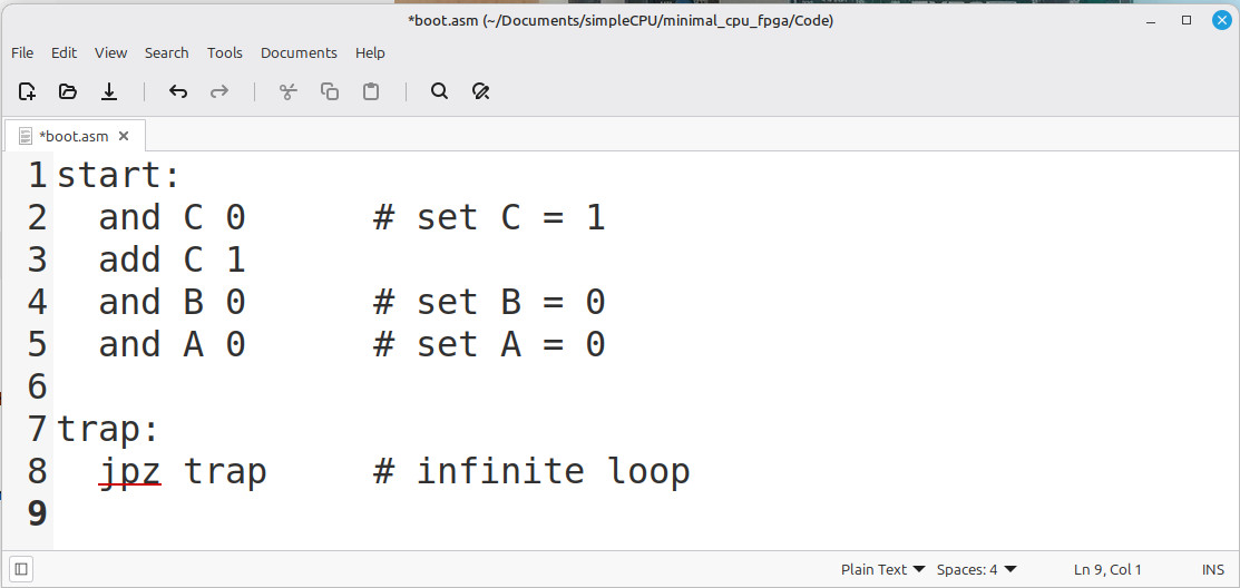

Figure 35 : Boot code, boot.asm (top) and boot.dat (bottom)
To run this program move toggle switch 0 into the 1 position i.e. enable the minimalCPU, then move toggle switch 3 into the 0 position i.e. remove the reset signal, 5mm GREEN LED off. These two steps are shown in figures 36 and 37. When the reset signal is set to a logic 0 the minimalCPU will execute the program shown in figure 35, the 5mm RED LED will turn on each time it's clock signal is in the logic 1 / high state. The four small green LEDs above the toggle switches will display the address of the instruction being executed i.e. show the binary patterns 0 to 4, the final LED states are shown in figure 38. To rerun this program move toggle switch 3 into the 1 position, then back to the 0 position i.e. pulse the minimalCPU's reset signal.
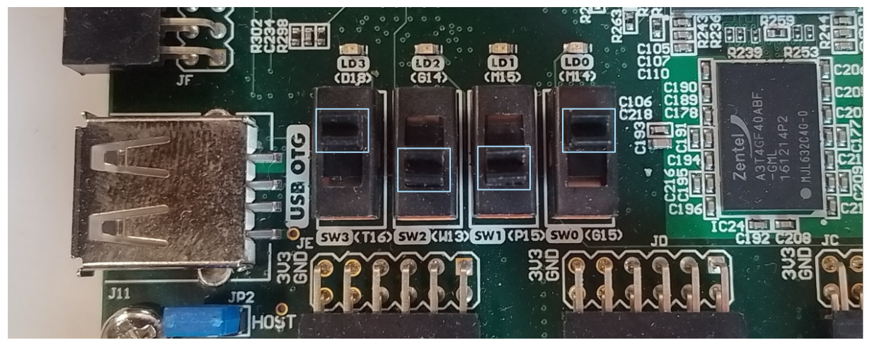
Figure 36 : MinimalCPU reset and enabled.
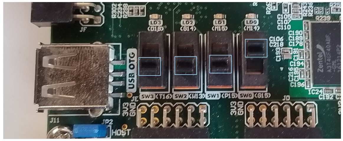
Figure 37 : MinimalCPU enabled.
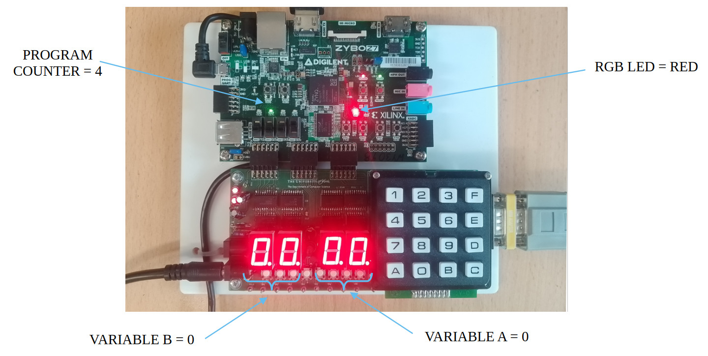
Figure 38 : Final state of FPGA LEDs.
Examine figures 35 and 38, can you see why the four small green LEDs are displaying the value "0100" and why the RGB LED is red?
To execute different programs you can access the minimalCPU's code_memory using a serial terminal i.e. the monitor component. Connect the FPGA board to the PC using the serial cable in the desk draw. Plug the 9-way D-sub connector (DE-9) and the orange adaptor into the FPGA board, then plug the USB-to-Serial adaptor on the other end of the cable into the PC, as shown in figure 39.
Note, to fully understand how to use the serial monitor you need to know the commands supported by MikeMon, the monitor code, for more info: (Link), however, for simple commands just follow the examples below.
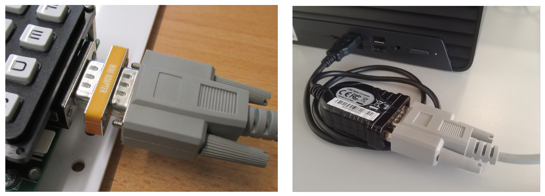
Figure 39 : Serial lead.
Under Windows the COM port assigned to the USB-to-Serial adapter can vary depending on what other devices have been connected to the PC. Normally it is COM6, but to identify this COM port open Device Manager i.e. type "Device Manager" into the search box and run this application. A pop-up window will appear informing you that you can only view these device settings, click OK. Then expand the Ports (COM & LPT) section, as shown in figure 40, and identify the COM port of the Prolific USB-to-Serial device e.g. in this example it has been assigned COM6.
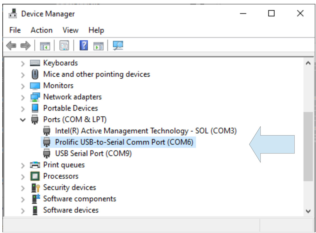
Figure 40 : Device Manager.
The serial ASCII characters can be displayed on the PC using the terminal program PUTTY. This program monitors the PC’s serial port displaying any received ASCII characters and transmits back to the FPGA board any keyboard characters pressed. To run this program type "PuTTy" into the search box and run this application. The "PuTTy Configuration" window will now open, as shown in figure 41, click on the Serial radio button, then set Serial line (port): COM6 (this may vary) and Speed (baud rate): 9600, then click on Open.
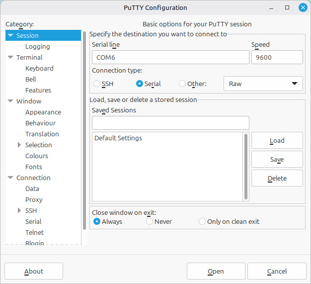
Figure 41 : Putty.
To confirm that the serial port is working correctly left click on the terminal window and press the escape key (ESC), you should see "MikeMon" and "\" character displayed, as shown in figure 42. If not check your connections.
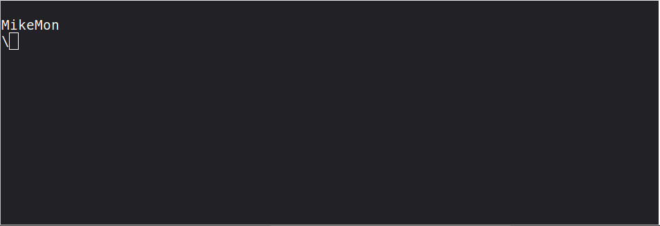
Figure 42 : MikeMon welcome banner.
To view the contents of the minimalCPU's code_memory enter the read command "0.FF" into the terminal, followed by the Enter key. This will print the minimalCPU's instruction memory to the terminal, as shown in figure 43. For more information on the different types of read and write commands supported by MikeMon: (Link).
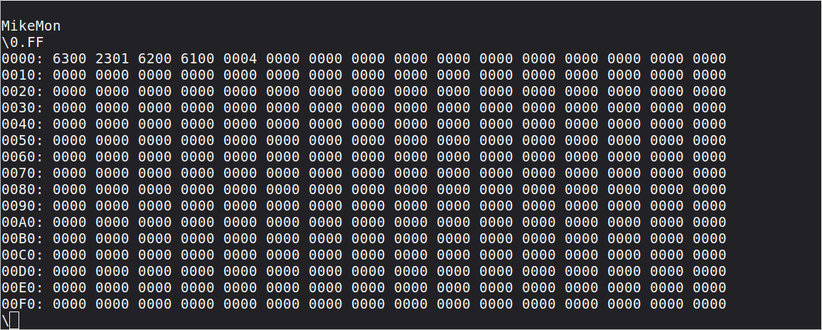
Figure 43 : Code Memory contents.
Move toggle switch 3 into the 1 position i.e. reset the minimalCPU, the 5mm GREEN LED will turn on. We can now update an instruction in code_memory i.e. change the number stored in variable C. In the serial terminal enter the write command "1:2302". This will change the instruction at address 1 from ADD C 1 to ADD C 2. You can confirm that this write command was successful by entering the read command "0.F", as shown in figure 44. To run this new program move toggle switch 3 into the 0 position i.e. remove the reset signal. What colour does the RGB now display, is it green? Do you understand why it has changed from red to green? Could you change this instruction again to make the RGB LED blue?

Figure 44 : Write and read commands.
In addition to modifying programs we can also upload new programs i.e. overwrite the boot.asm code. To shown how this can be done we can upload the test.asm program in figure 4. Again, move toggle switch 3 into the 1 position to reset the minimalCPU. Then either assemble the test.asm program to generate the test.mon file, or you can download it here: (test.mon). Open this file and cut and paste these characters i.e. address and machine code data, into the terminal, as shown in figure 45. To confirm this code was uploaded correctly you can enter the read command "0.1F", as shown in figure 46.
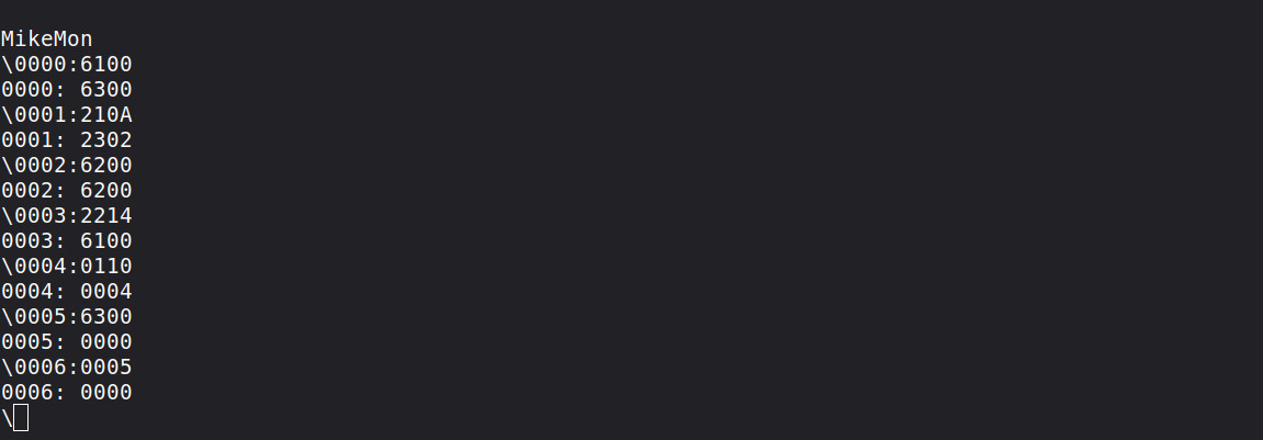
Figure 45 : Cut and paste programs.

Figure 46 : Check program uploaded ok
To run this new program move toggle switch 3 into the 0 position i.e. remove the minimalCPU reset, this program will now run updating the values displayed on the seven segment displays, as shown in figure 47. Do you understand why these values were displayed i.e. A=0x1E and B=0x14?
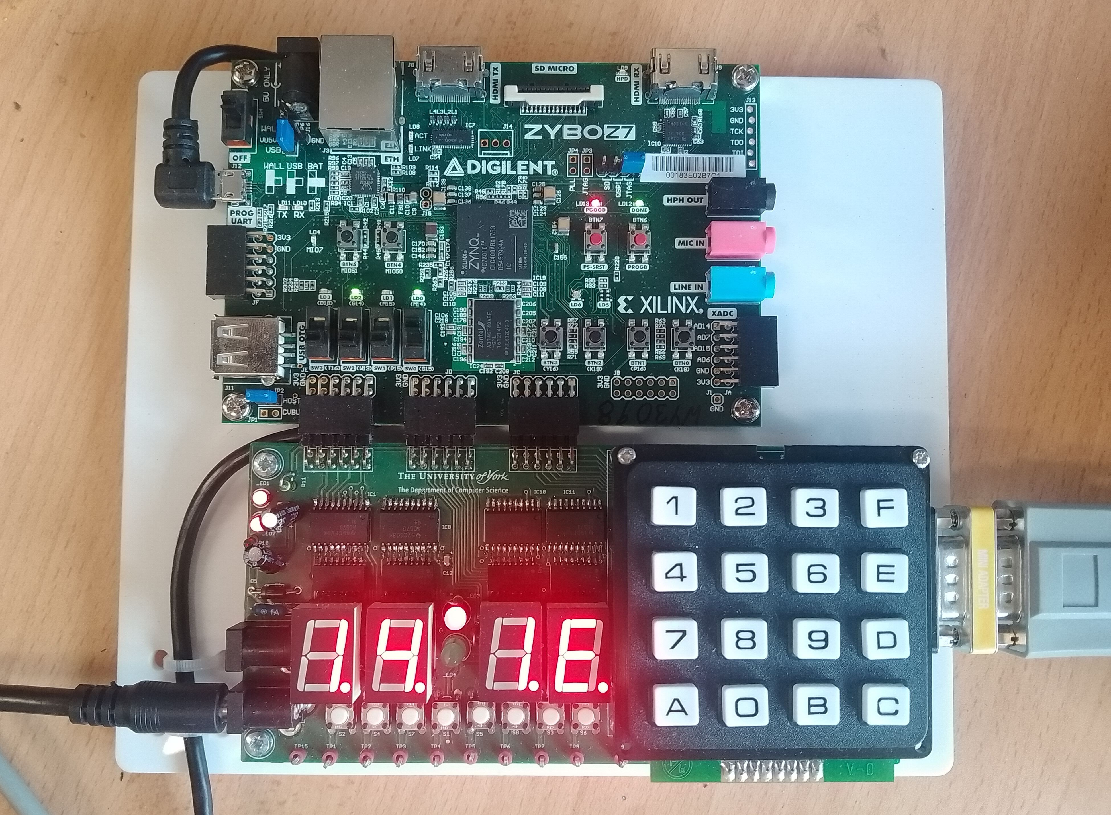
Figure 47 : FPGA seven segment values
Using the minimalCPU instruction-set simulators (Link), or the FPGA board test out your solutions to the following questions:
Q1) initialise the variables A and B with the values:
          128  64  32  16  8  4  2  1
A = 14 =  0    0   0   0   1  1  1  0
B = 35 =  0    0   1   0   0  0  1  1
Next, consider the program below, what is the final value stored in variable A?
ADD A B
AND A B
Hint, remember that the first variable i.e. A in this example, is overwritten with the result.
Q2) write a program to perform the following calculation:
A = A * 5
Hint, what is multiplication? You will need to use multiple instructions to implement the multiply function. Test your solution by setting variable A to 10 i.e. 0x0A, generating the result 50 i.e. 0x32.
Q3) write a program to perform the following calculation. Your solution must use less than eight instructions.
A = A * 16
Hint, accumulated additions. Test your solution by setting variable A to 10 i.e. 0x0A, generating the result 160 i.e. 0xAD.
Q4) write a program to perform the following calculation i.e. the multiplication of two unknown variables.
A = A * B
Hint, you will need to use the JPZ jump instruction. Jumps are made to labels within a program i.e. a name (label) ending with a ":". Consider the example below, the JPZ instruction jumps to the label START if the result of the ADD instruction produces a zero result, otherwise the next instruction in the program is executed i.e. this code gets stuck in an infinite loop.
START:                    START:
   AND X 0                   X=0
   AND Y 0                   Y=0
   ADD X Y                   X=X+Y
   JPZ START                 IF RESULT = 0 THEN START
   ADD Z X                   Z=Z+X

This work is licensed under a Creative Commons Attribution-NonCommercial-NoDerivatives 4.0 International License.
Contact email: mike@simplecpudesign.com