In the being there was the simpleCPU (Link), this evolved into simpleCPU_v1a (Link), moved out of the FPGA and onto bread-board (Link), to complete the circle i have taken the bread-board implementation and ported this back to FGPA. Why? Well, i do confess the previous ISE schematics were a little on the messy side. In the original design i put too much on each circuit diagram, which added a lot of visual clutter and made them tricky to read. Therefore, to hopefully remedy this ive redrawn them to make things easier to see. As much as possible this version is direct copy of the bread-boarded version. The main difference is that the memory used is dual-port i.e. has a separate uni-directional input and output data buses, unlike the bi-directional data bus used in the bread-board version. The reason for this change is as previously discussed in the bread-board design notes i.e. lack of and disadvantages of tri-state drivers. Previous discussion of these processors have been from the bottom-up point of view i.e. logic gates to systems, to add a bit of variety the discussion below is a top-down dive into the simpleCPU's architecture.
TOP : top level, the computer
CPU : processor
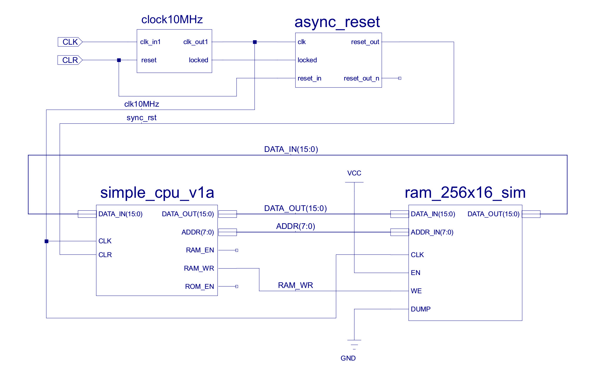
Looking at figure 1 you can see that this is a basic Von Neumann architecture: one processor and one memory. This schematic shows the external interfaces of each component i.e. pins, you should also be able to identify the main buses (thinker lines) and control signals (thinner lines) used to transfer information between these devices. In addition to these two main components you have the clock and reset generators, these will be device (FPGA) specific. This computer does not have any inputs or outputs, so version 1 is for simulation / testing only i.e. it only has two inputs, the external clock (CLK) and reset line (CLR). We will add IO later.
The new and improved ISE project files for this computer can be downloaded here: (Link).
Figure 1 : the computer
This computer was developed for the two main teaching FPGA boards we use, the Digilent Zybo Z7: Zynq-7000 and the Arty A7: Artix-7, as shown in figure 2, but any FPGA will do, you would just need to modify the clock, memory and IO interface.
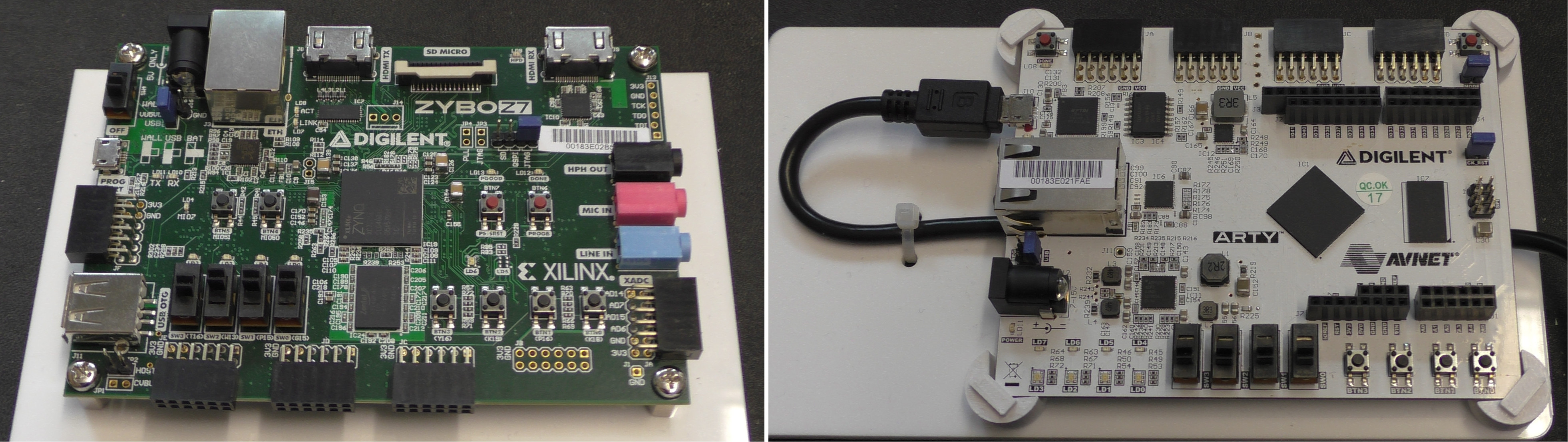
Figure 2 : FPGA boards
Each board has an on-board oscillator, generating signal CLK. The output clock frequency of these boards varies from 100MHz to 125MHz. If we were to use a clock in this range, the output signals used to drive external pin would look a little noisy when viewed on an external scope or logic analyser i.e. the joys of transmission lines. Therefore, so that signals look a little more squarer we need to scale this clock signals down to a slower speed e.g. 1 - 10MHz. To do this you can use the Xilinx IP-Core generator, as shown in figure 3. This wizard will automatically generates the schematic component CLOCK10MHz which uses the on-chip clock generator hardware to produce the required 10MHz system clock. Note, this is a teaching processor, not looking for raw processing performance.
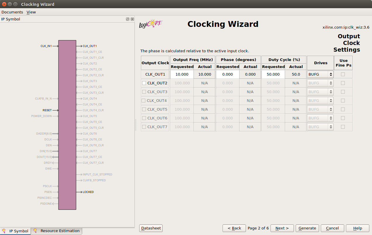
Figure 3 : FPGA clock generator
With any oscillator it takes a little while i.e. a few milli seconds / cycles for the oscillator to settle down to the correct frequency. During this time you don't want the computer to run, as it will be operating with an unstable clock, which could lead to unanticipated and undesirable outcomes. Therefore, the clock generator has a LOCKED output to indicate when the output clock is stable. This signal is combined with the external reset (CLR) in the ASYNC_RESET component, converting the external asynchronous reset signal (from the push button) to a synchronous reset used to initialise the processor. I could of implemented this component as a schematic, but for the sake of speed i implemented it in VHDL (a textual hardware description language), as shown below:
-- =============================================================================================================
-- *
-- * Copyright (c) Mike
-- *
-- * File Name: clock_10MHz.vhd
-- *
-- * Version: V1.0
-- *
-- * Release Date:
-- *
-- * Author(s): M.Freeman
-- *
-- * Description: 10MHz clock wrapper
-- *
-- * Conditions of Use: THIS CODE IS COPYRIGHT AND IS SUPPLIED "AS IS" WITHOUT WARRANTY OF ANY KIND, INCLUDING,
-- *                    BUT NOT LIMITED TO, ANY IMPLIED WARRANTY OF MERCHANTABILITY AND FITNESS FOR A
-- *                    PARTICULAR PURPOSE.
-- *
-- * Notes:
-- *
-- =============================================================================================================


library IEEE;
use IEEE.STD_LOGIC_1164.ALL;

entity async_reset is
Port ( clk         : in  STD_LOGIC;
       locked      : in  STD_LOGIC;
       reset_in    : in  STD_LOGIC;
       reset_out   : out STD_LOGIC;
       reset_out_n : out STD_LOGIC );
end async_reset;

architecture async_reset_arch of async_reset is

    constant SIZE : integer := 4;

    signal reset_internal : std_logic_vector(SIZE downto 0);
    signal full : std_logic_vector(SIZE downto 0);

begin

    full <= (others => '1');

    reset_shift_reg : process ( clk, reset_in )
    begin
        if reset_in = '1'
        then
            reset_internal <= (others =>'0');
        elsif clk='1' and clk'event
        then
            if locked = '1'
            then
                reset_internal(0) <= '1';

                for I in 0 to SIZE-1
                loop
                    reset_internal(SIZE-I) <= reset_internal(SIZE-I-1);
	            end loop;
	         else
	           reset_internal <= (others =>'0');
	         end if;
	     end if;
    end process;


    reset_gen : process( clk )
    begin
        if clk='1' and clk'event
        then
            if reset_internal /= full
            then
                reset_out   <= '1';
                reset_out_n <= '0';
            else
                reset_out   <= '0';
                reset_out_n <= '1';
            end if;
        end if;
    end process;

end async_reset_arch;
Basically, this hardware holds the processor in a reset state until the oscillator raises the LOCKED input signal. It then holds the processor in this reset state for a specified number of clock cycles i.e. the parameter SIZE, before releasing the reset signal (setting it low) allowing the processor to fetch the first instruction. This functionality is re-triggered if the external reset button is pressed.
The ISE schematic symbol for the simpleCPU processor is shown in figure 4. The ISE tools support hierarchical design, such that if you highlight a component/symbol and click on the "push" icon you can move into that component i.e. a sub-circuit, as shown in figure 5.
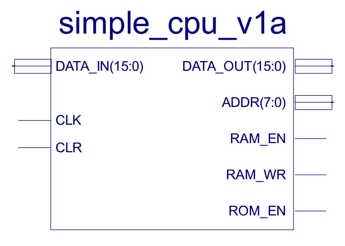
Figure 4 : CPU symbol
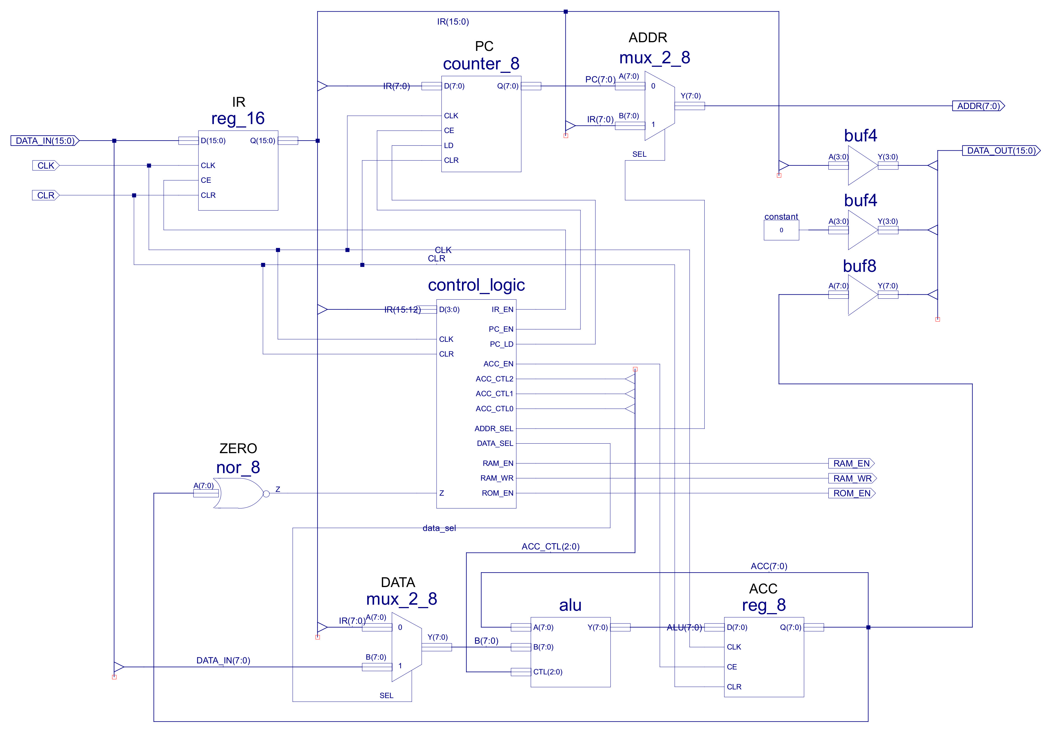
Figure 5 : CPU circuit diagram
The circuit diagram shown in figure 5 implements the same architecture as the previous bread-board implementation (Link), however, there are a couple of tweaks, as we are no longer constrained by the limitations of each SPLD and we are not using a bi-directional data bus. One point of possible confusion is how the DATA_OUT bus is driven i.e. the 16bit output is connected to two 4bit buffers and one 8bit buffer as follows:
DATA_OUT(15 downto 12) = IR(11 downto 8)
DATA_OUT(11 downto 8)  = "0000"
DATA_OUT(7 downto 0)   = ACC(7 downto 0)
As discussed in the assembler documentation instruction bits (11 downto 8) are not normally used by the CPU's hardware. Therefore, these can be set to any value and will not affect the operation of the processor. Knowing this we can use this to our advantage to implement additional functionality, described later in the "Improvised instructions" section.
Ignoring this small twist for the moment, this FPGA implementation does have the same basic design as that shown in figure 6. Comparing the circuit and block diagram you should be able to match the main architectural components:
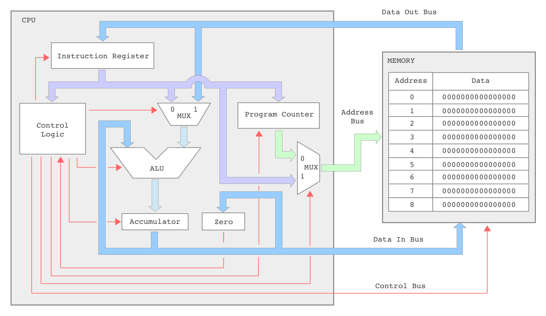
Figure 6 : CPU block diagram
Again, thick lines in the circuit diagram indicate busses i.e. a collection of wires, either 16 bit or 8 bit wide. Thin lines control signals i.e. single wires, bits. This is the main difference between a block diagram and a circuit diagram, you start to get a little bit more clutter with all the wires required to actually implement the computer. Moving to a block diagram does simplify the view, but you should always remember that hidden from view is awful lot of wire, as shown in the bread-board version shown in figure 7, you are looking at approximately 400 - 500 wires to implement the required buses and control signals.
Note, the control signals RAM_EN and ROM_EN are not used as the FGPA implementation does not use separate RAM and ROM components.
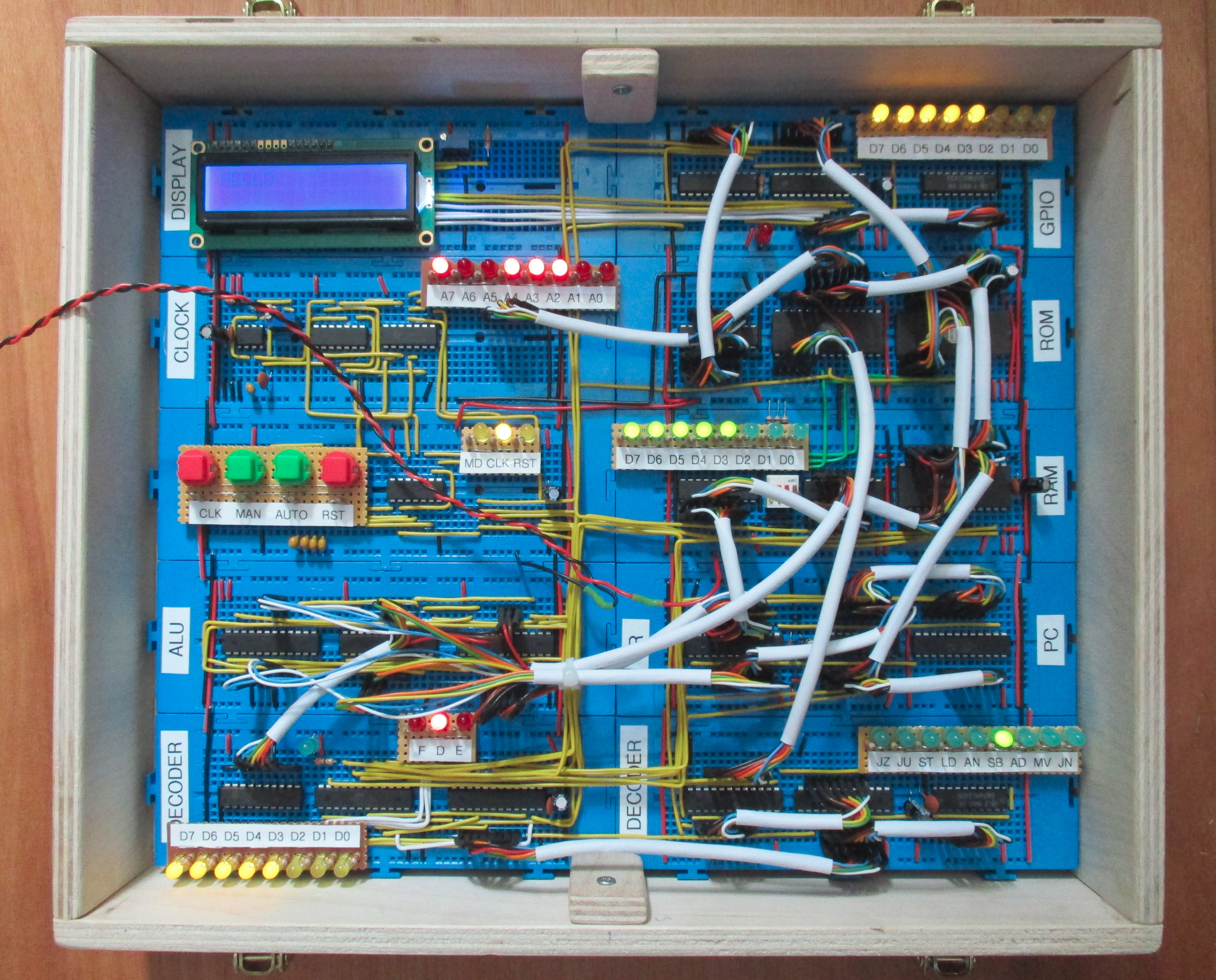
Figure 7 : CPU bread-boarded computer
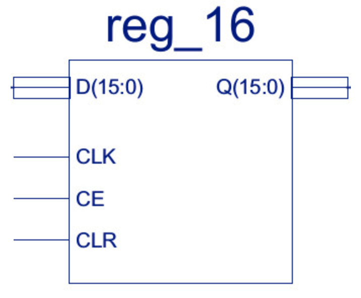
Figure 8 : Instruction register
The Instruction Register (IR) is used to hold the instruction currently being processed by the processor. A simple 16bit register i.e. 16 flip-flops, updated in parallel, with clock enable and asynchronous clear. If the CE line is high the register is updated on a rising clock edge. The register's CLR input is independent of the clock state i.e. asynchronous, setting the register to zero when the CLR is high. From an implementation view point this register is broken down into two 8bit registers, that are in turn broken down into two 4bit registers are shown in figure 9abc.
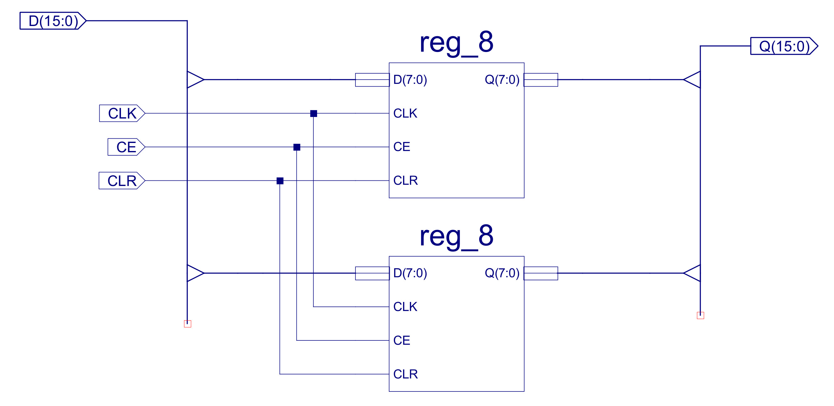
Figure 9a : 16 bit register
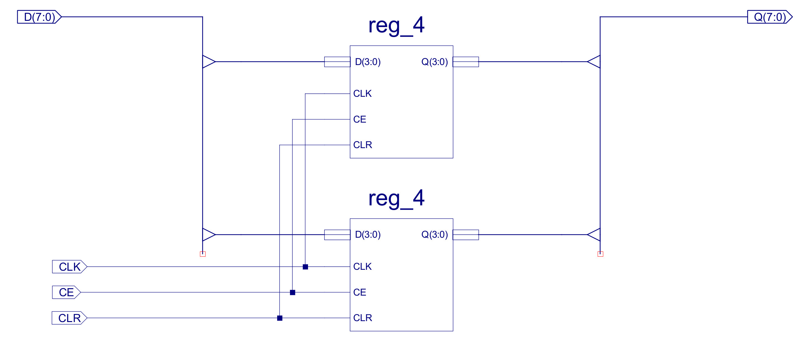
Figure 9b : 8 bit register
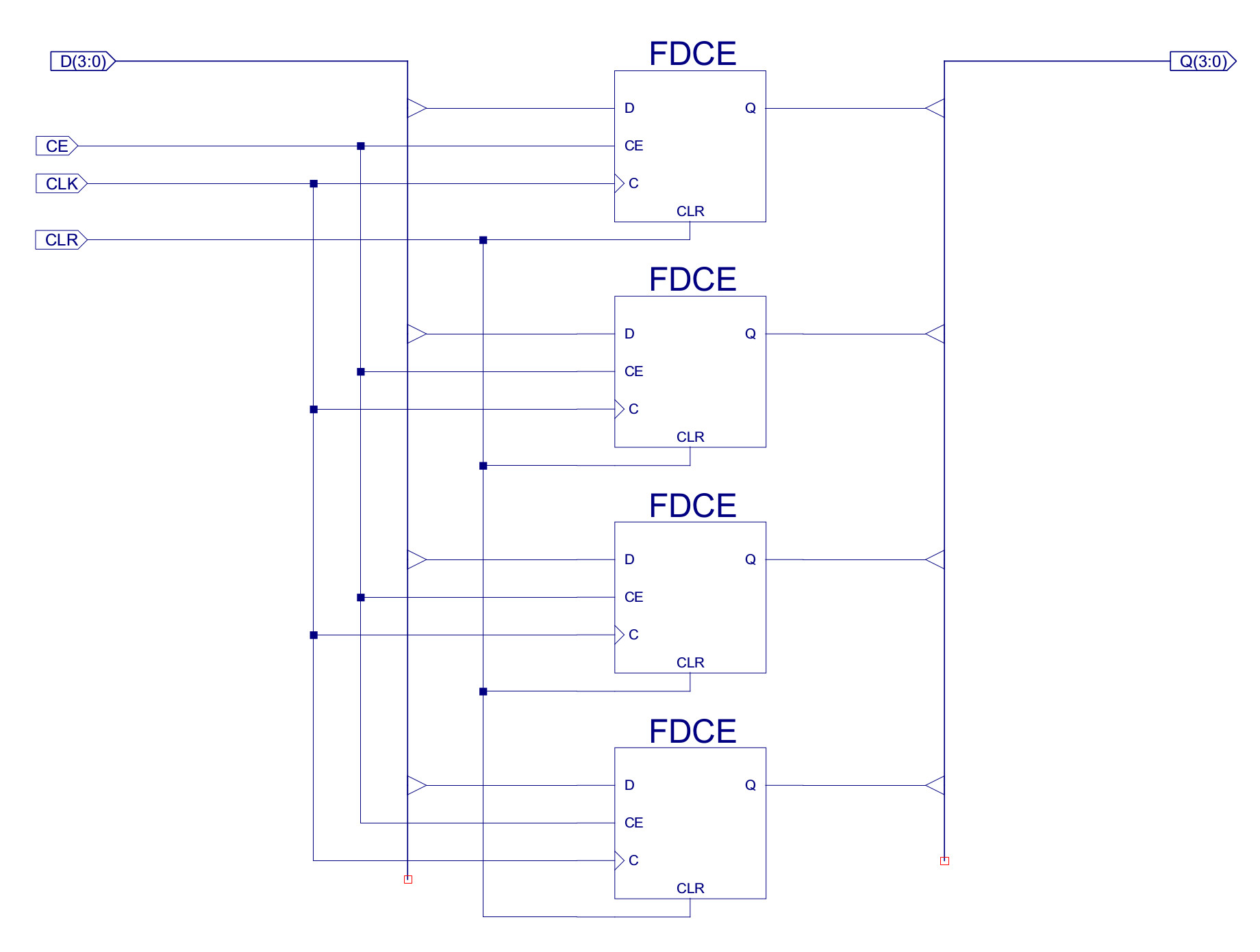
Figure 9c : 4 bit register
Note, the 16bit register could of been implemented in one schematic containing 16 flip-flops, the reason for breaking this component down into 8bit and 4bit registers was to help remove clutter and make the schematics easier to read i.e. to make the schematics simpler and smaller. A second reason was to increase component reuse e.g. the 8bit register component is used in the ACC and PC.
The IR CE line is only enabled during the FETCH phase, updating the register with the accessed 16bit instruction. A simulation of the IR being updated is shown in figure 10, in which you can see that the CE is set by the control logic on the first rising edge, triggering the registers update on the second.
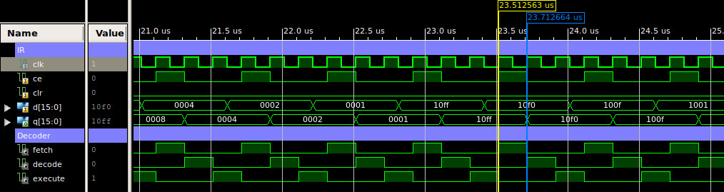
Figure 10 : IR timing waveform
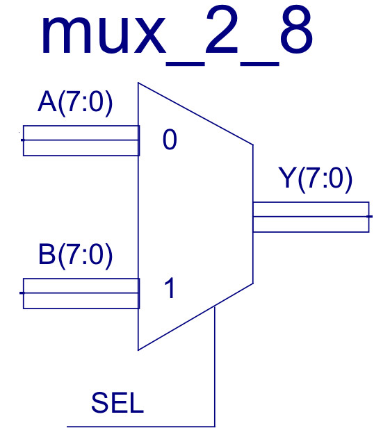
Figure 11 : Multiplexer
There are two top level multiplexers (MUX): Data-mux and Address-mux. Constructed from eight two-input multiplexers, as shown in figure 12, allowing the control unit to select between two 8bit buses e.g. the ADDR multiplexer selects between the PC and the absolute address stored in the IR. If sel=0 the A input is routed to the output Y, else if sel=1 the B input is routed to the output Y. Note, these multiplexers are described in more detail in the simpleCPUv1 documentation (Link)
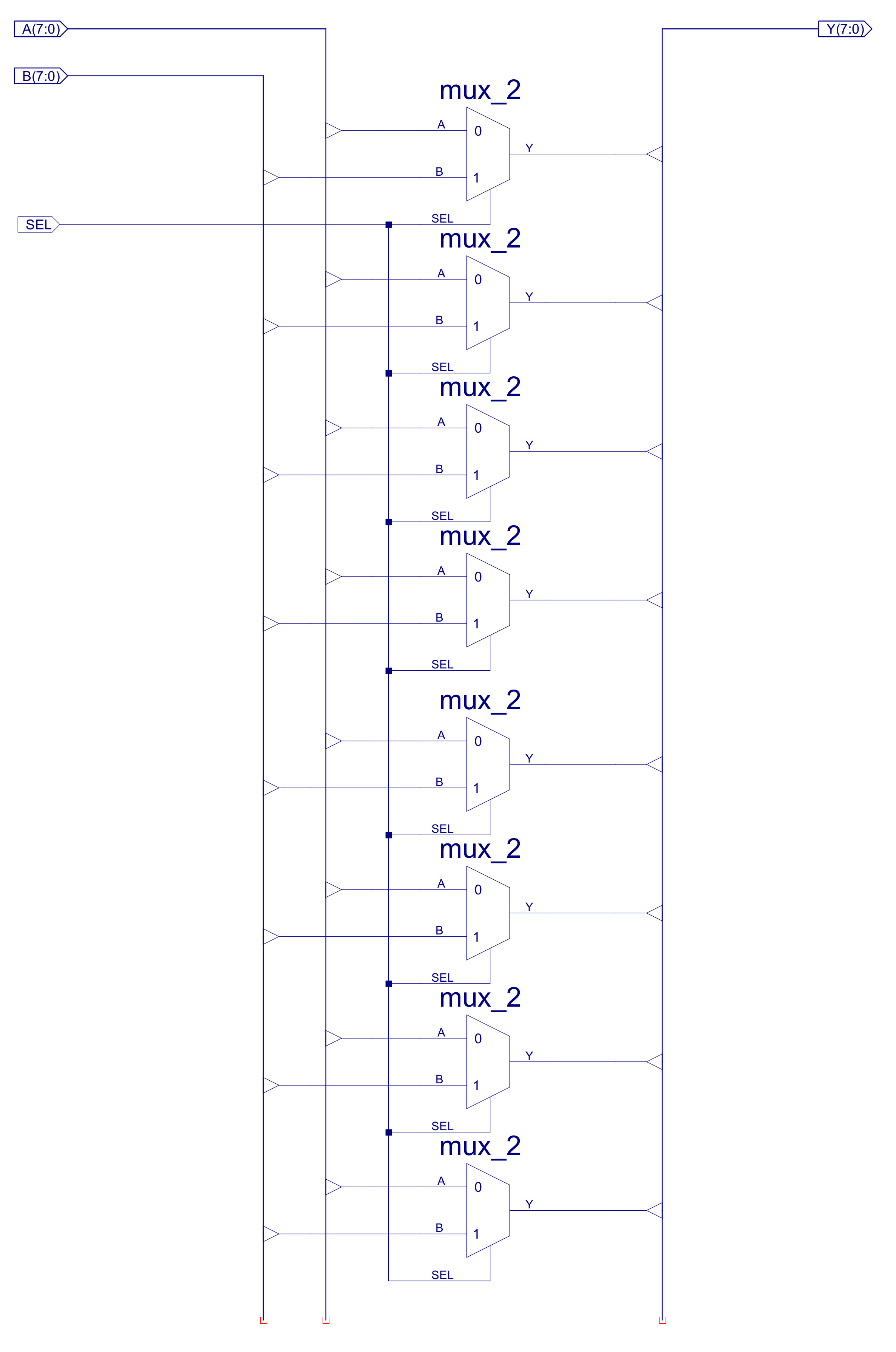
Figure 12 : Multiplexer circuit diagram
A simulation of the ADDR and DATA multiplexers is shown in figure 13.
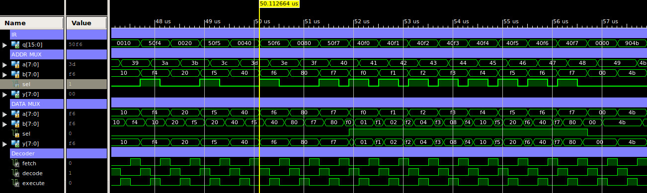
Figure 13 : Multiplexer timing diagram
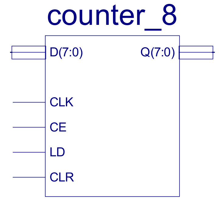
Figure 14 :Program counter
The Program Counter (PC) holds the address of the current instruction being processed. This eight bit loadable binary counter stores the 8bit address used in the FETCH phase. As with the IR this component has active high clock enable (CE) and clear (CLR) lines. Data to be loaded into the counter e.g. during a JUMP instruction, is placed on the D inputs. If the counter's CE and LD lines are set high, on the next rising clock edge the D input data is loaded onto the Q outputs. If the CE is high and LD is low, the counter is incremented. From an implementation view point this counter is broken down into an 8bit register, 8bit adder and an 8bit multiplexer, as shown in figure 15.
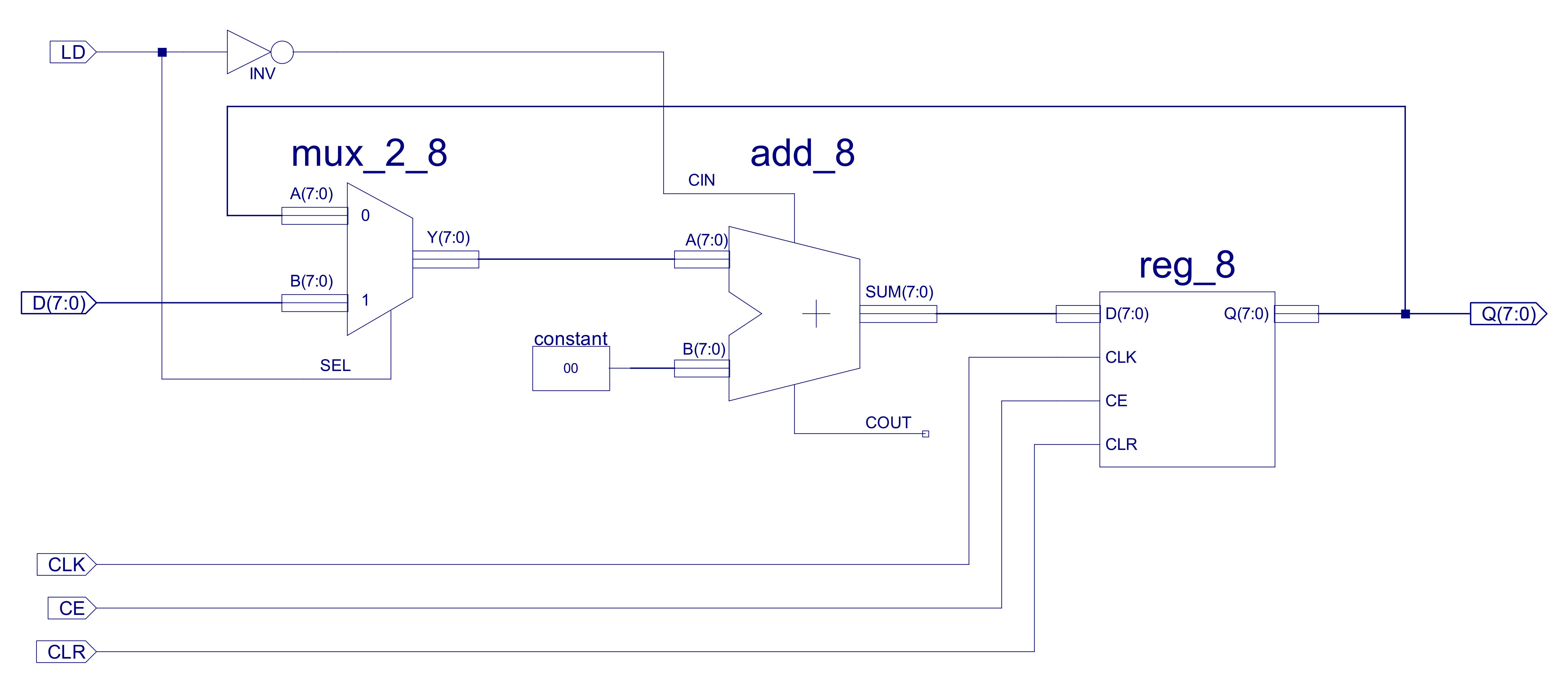
Figure 15 : Program counter circuit diagram
In normal operation the PC value is stored in the 8bit REG_8 component, as shown in figure 9b. Its D input is driven by the 8bit adder (we will look into the adder in more detail in the ALU section). The adder is used as an incrementer, input A is driven by the multiplexer, routing the PC value back round. Input B of the adder is hardwired to the constant 0. The CIN input of the adder is connected the inverted LD signal. Therefore, if LD=0, CIN will be driven to 1, incrementing the PC value. If CE=1, on the next rising edge the REG_8 component is updated with the incremented value. If LD=1, the counter is loaded with the value on its D input, the multiplexer switches the adder's A input from the PC value to the D input. If LD=1 the adder's CIN line is set to 0, therefore, if CE=1, on the clock's rising edge the REG_8 component is updated to the new value: D + 0 i.e. D is transferred through the adder unaltered. A simulation of the program counter performing increment and load operations is shown in figure 16.
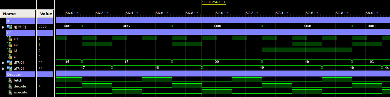
Figure 16 : PC timing waveform
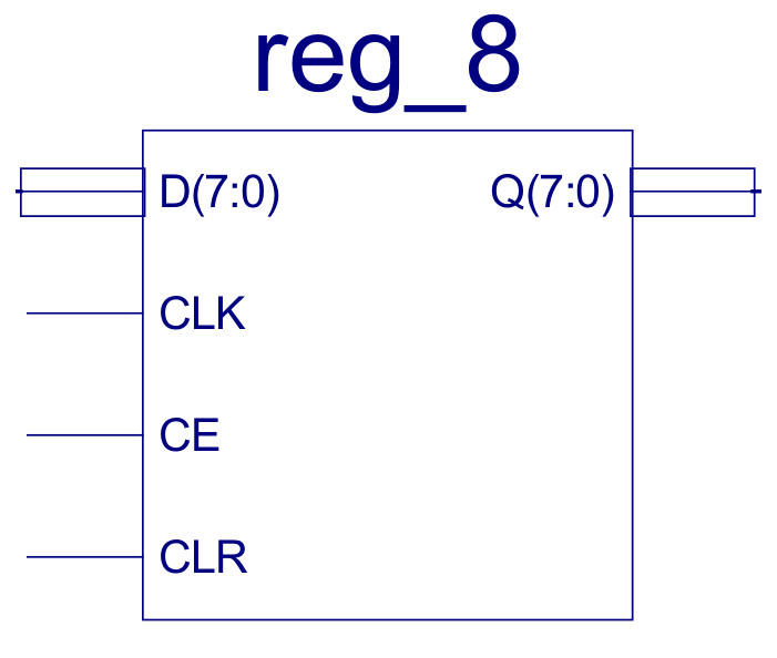
Figure 17 : Accumulator
The Accumulator (ACC) is a general purpose data register that is used to store operand data loaded from memory, or intermediate results that have been calculated. An eight bit register, REG_8 component, shown in figure 9b, with clock enable and asynchronous clear. A simulation of the accumulator being updated at the end of the execution phase is shown in figure 18. Note, as this processor only has one data register, results stored in this register will need to be written back to memory before the next calculation can be performed i.e. the next calculation will need to overwrite the ACC with its result. Therefore, program variables will need to be moved in and out of the processor i.e. to and from external memory, using the LOAD and STORE instructions.
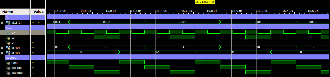
Figure 18 : ACC timing waveform
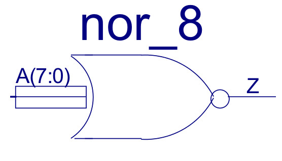
Figure 19 : Zero detect
To keep things simple on the simpleCPU conditional JUMP instructions are based on the state of the ACC i.e. does it contain a zero or a non-zero value. A very simple logic circuit, an 8 input NOR gate, its inputs are connected to the ACC output, produces a logic 1 when the ACC is zero. The implementation of this component is shown in figure 20. A simulation of the zero detect with the ACC containing both zero and non-zero results is shown in figure 21.
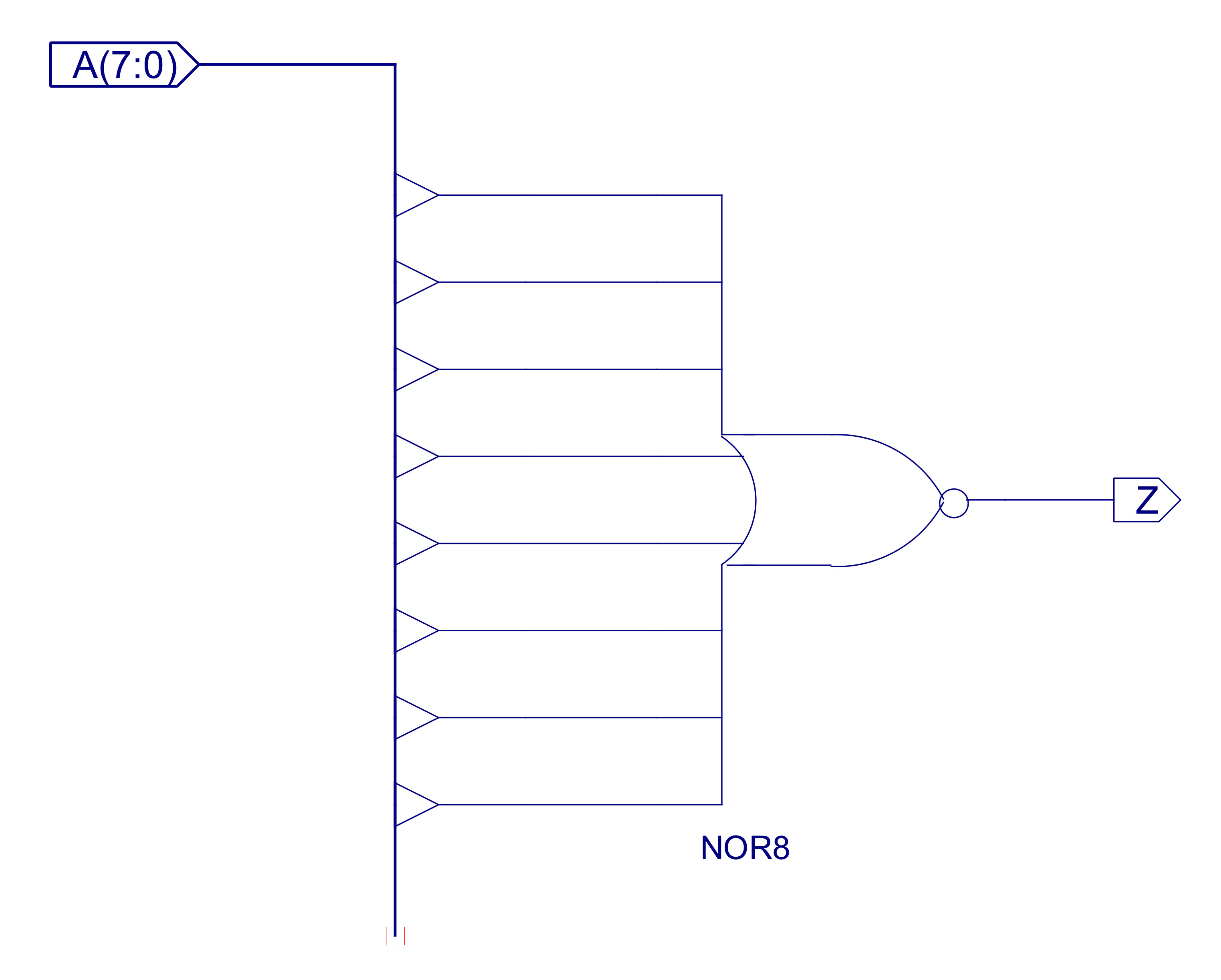
Figure 20 : Zero detect circuit diagram
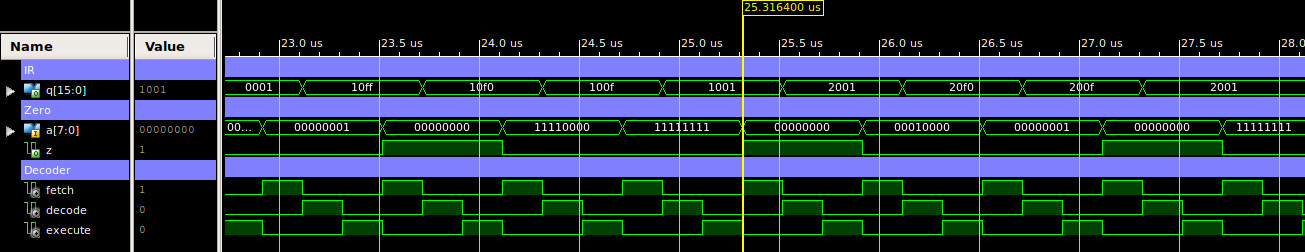
Figure 21 : Zero detect timing waveform
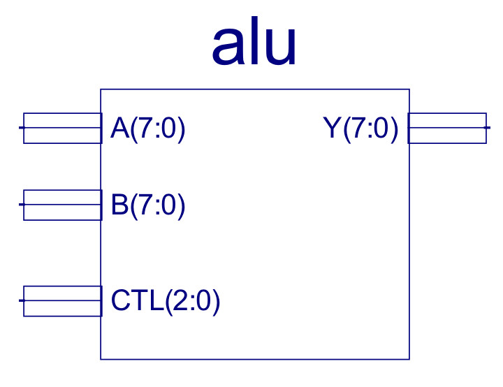
Figure 22 : Arithmetic and Logic Unit
The number crunching component within the processor. As this machine is an accumulator based architecture i.e. instructions define a single operand, the other operand is always the ACC and results produced by the ALU are always written back to the ACC. The ALU performs the core functions of the processor: add, subtract, bitwise-AND and data movement. From an implementation view point this component is broken down into an 8bit adder-subtractor, 8bit bitwise-AND and a three input 8bit multiplexer, as shown in figure 23.
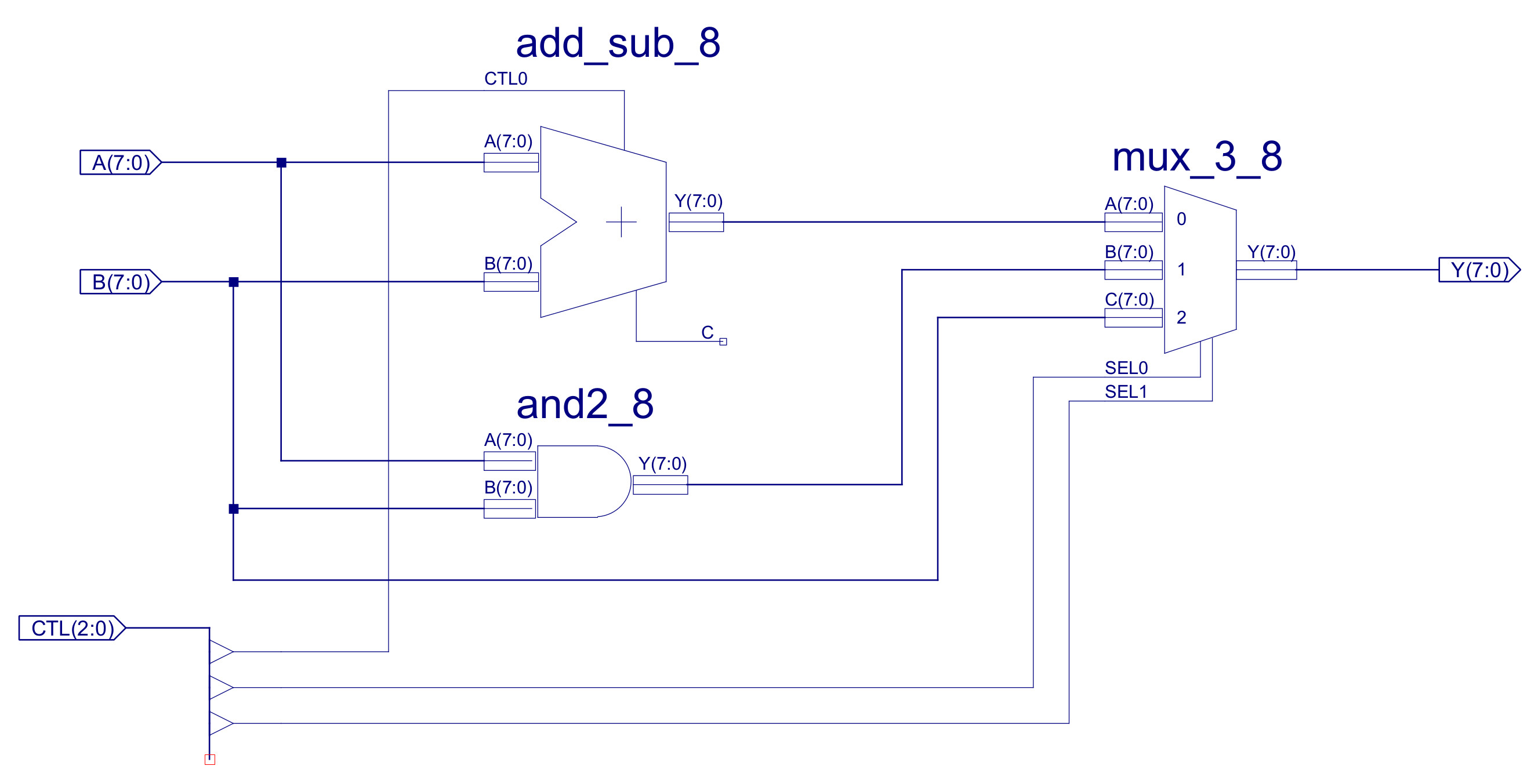
Figure 23 : ALU circuit diagram
The key building block of this and any processor is the adder: ADD_SUB_8, performing binary addition and subtraction. The internal implementation of this component is shown in figure 24. Subtraction is performed using 2s compliment addition. If CTL0=0 this component performs an ADD, the data on the B input is XORed with 0 i.e. is passed through unaltered, therefore Y=A+B. If CTL0=1 this component performs a SUBTRACT, the data on the B input is XORed with 1s i.e. each bit is inverted, CIN=1, therefore Y=A+(NOT B)+1. The implementation of the XOR_2 component is shown in figure 25. Note, remember when using 2s compliment: invert the bits and add 1, therefore, this hardware performs Y=A+(-B).
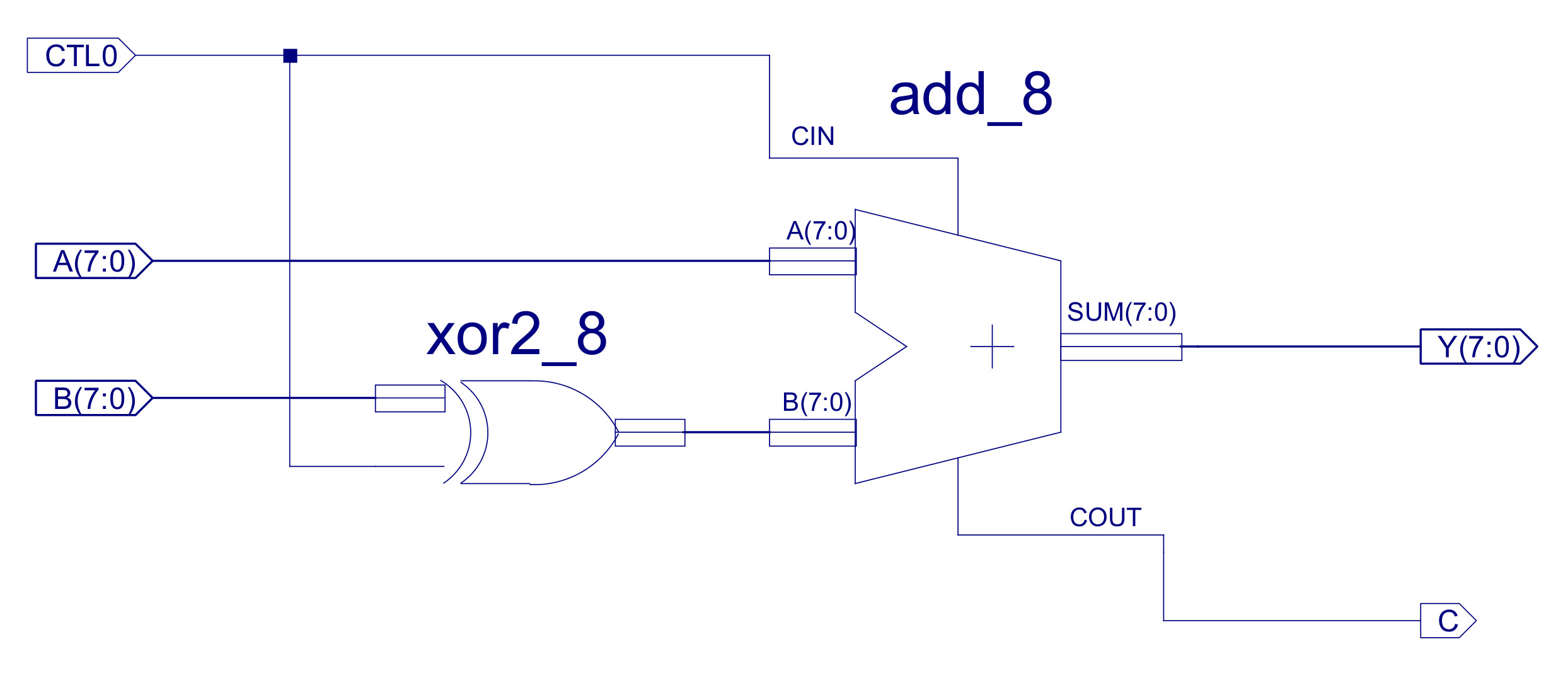
Figure 24 : ADD_SUB_8 circuit diagram
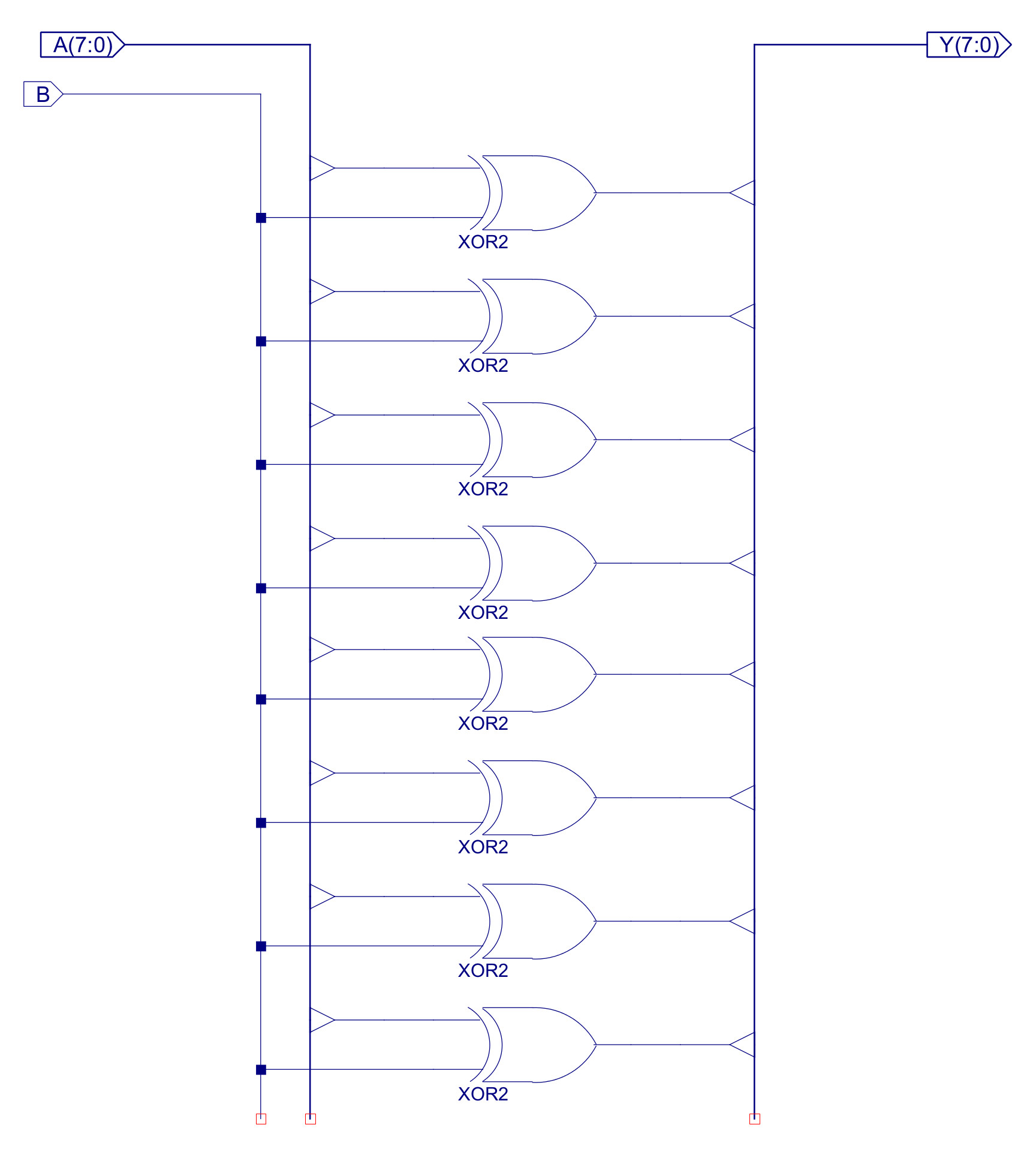
Figure 25 : XOR2_8 circuit diagram
The adder component ADD_8 is a basic ripple adder as previous described in the documentation for simpleCPUv1 (Link). Again, this component is broken down into a series of sub-components to simplify the schematics and improve readability, as shown in figures 26 - 29.
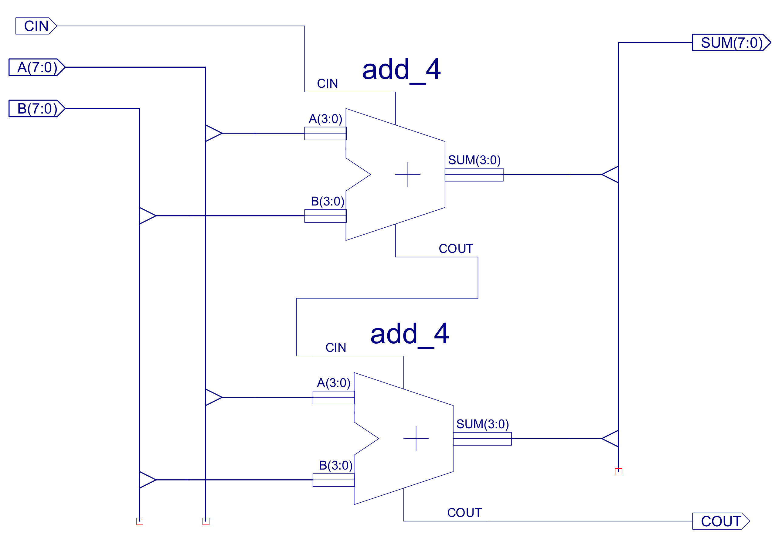
Figure 26 : ADD_8 circuit diagram
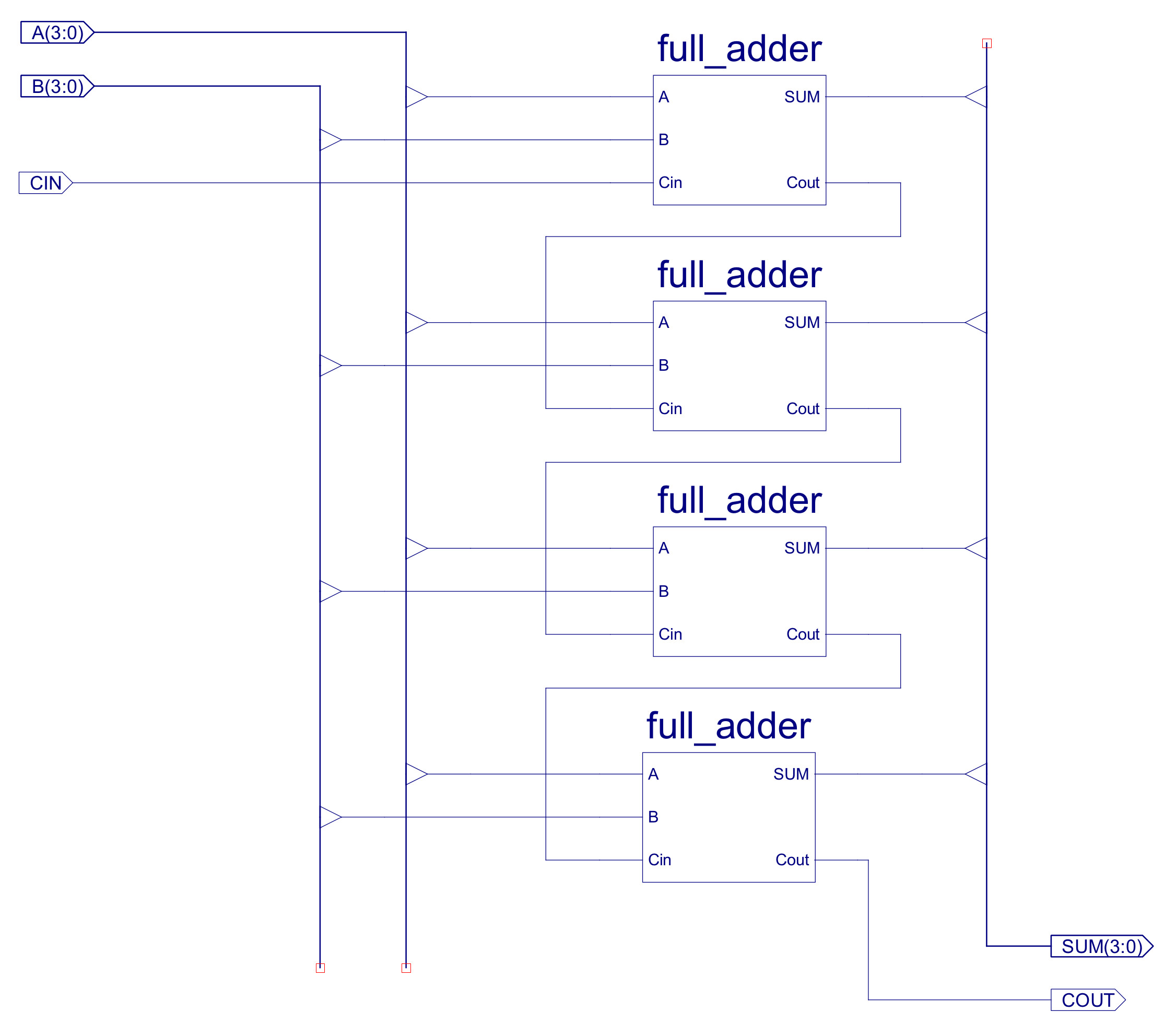
Figure 27 : ADD_4 circuit diagram
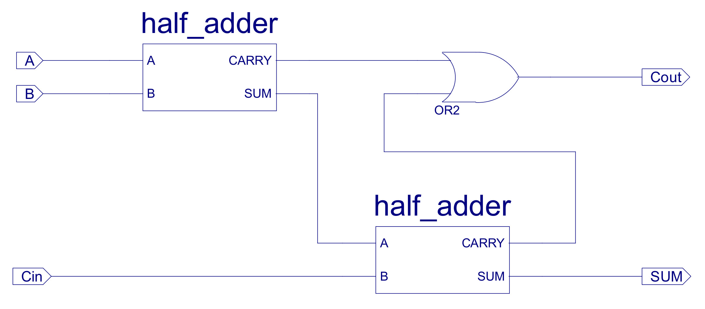
Figure 28 : FULL_ADDER circuit diagram
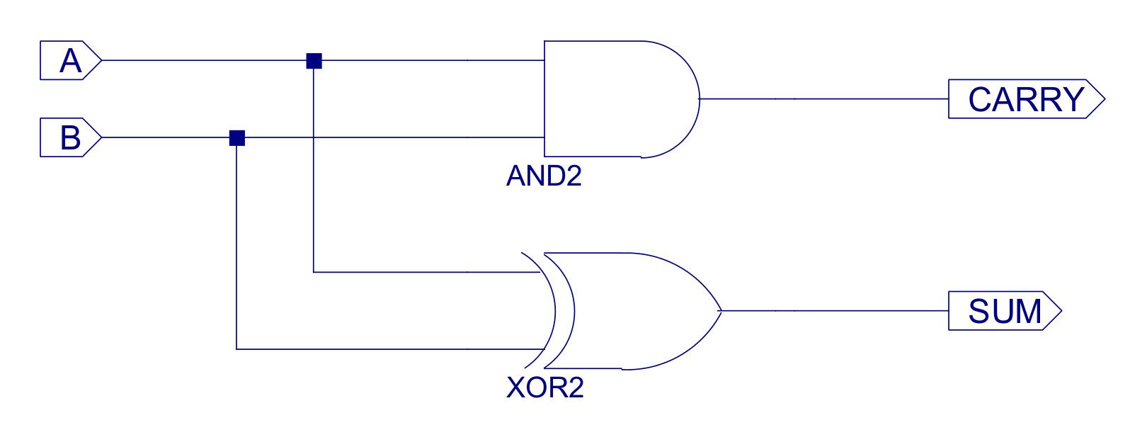
Figure 29 : HALF_ADDER circuit diagram
A simulation of the ALU performing move, addition and subtractions is shown in figure 30. Note, the IR, ACC and decode control signals are also shown to identify when these instructions are active.
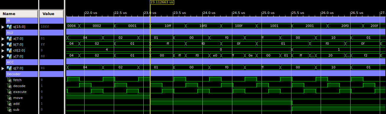
Figure 30 : ADD_SUB_8 timing diagram
The logical processing of this ALU is performed by the AND2_8 component which perform the bitwise-AND of the two operand. The implementation of this component is shown in figure 31, a simulation of the ALU perform bitwise-AND instructions is show in figure 32.
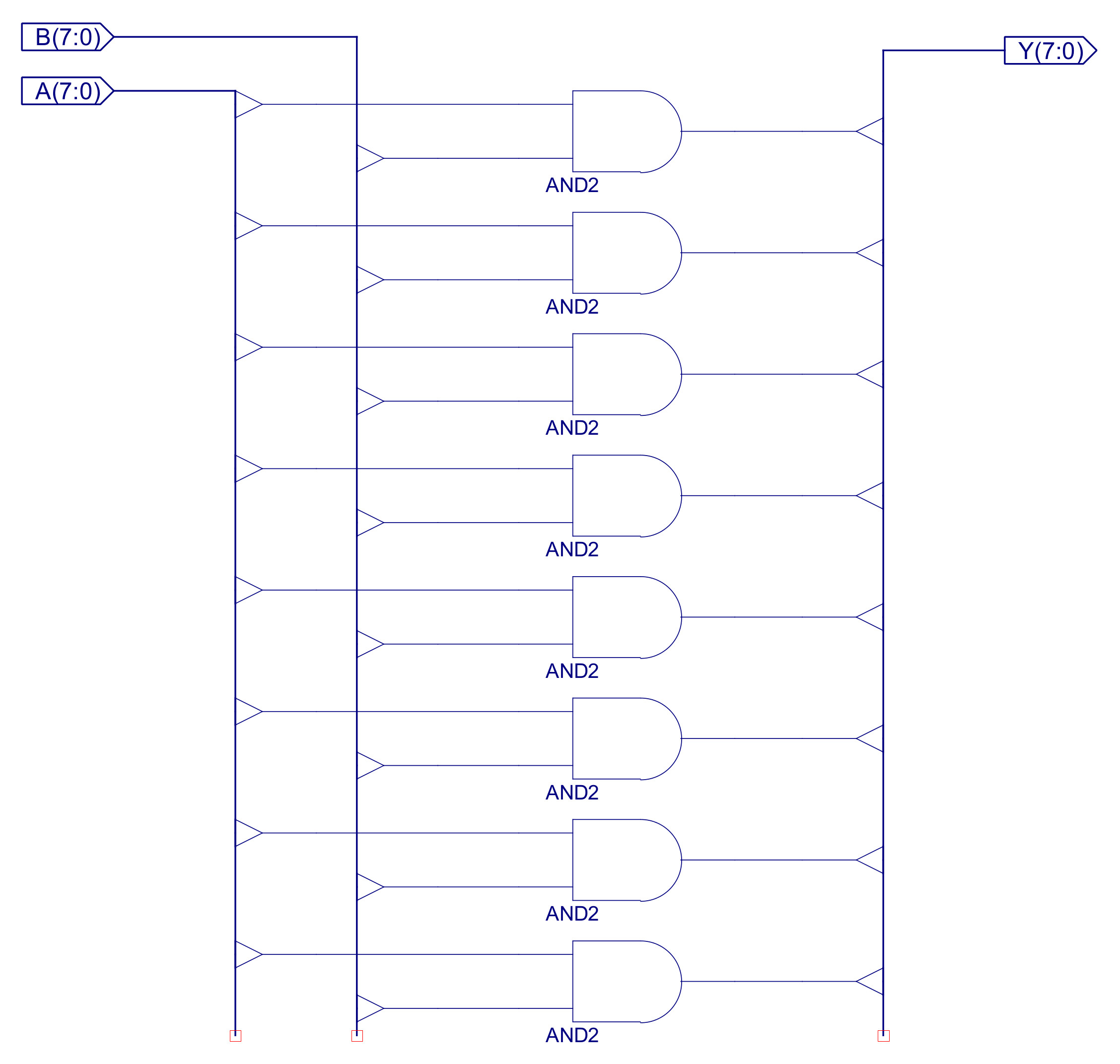
Figure 31 : AND2_8 circuit diagram
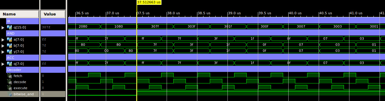
Figure 32 : AND2_8 timing diagram
Referring back to figure 23 you can see that both the adder and the bitwise-AND components work in parallel i.e. both are connected to inputs A and B, but only one of their outputs is passed to the Y output. This selection is performed by the MUX_3_8 multiplexer. This is implemented by the circuit shown in figure 33, using two of the MUX_2_8 components previously discussed. Note, input C performs a simple pass through function needed by LOAD and MOVE instructions i.e. reading memory or constant.
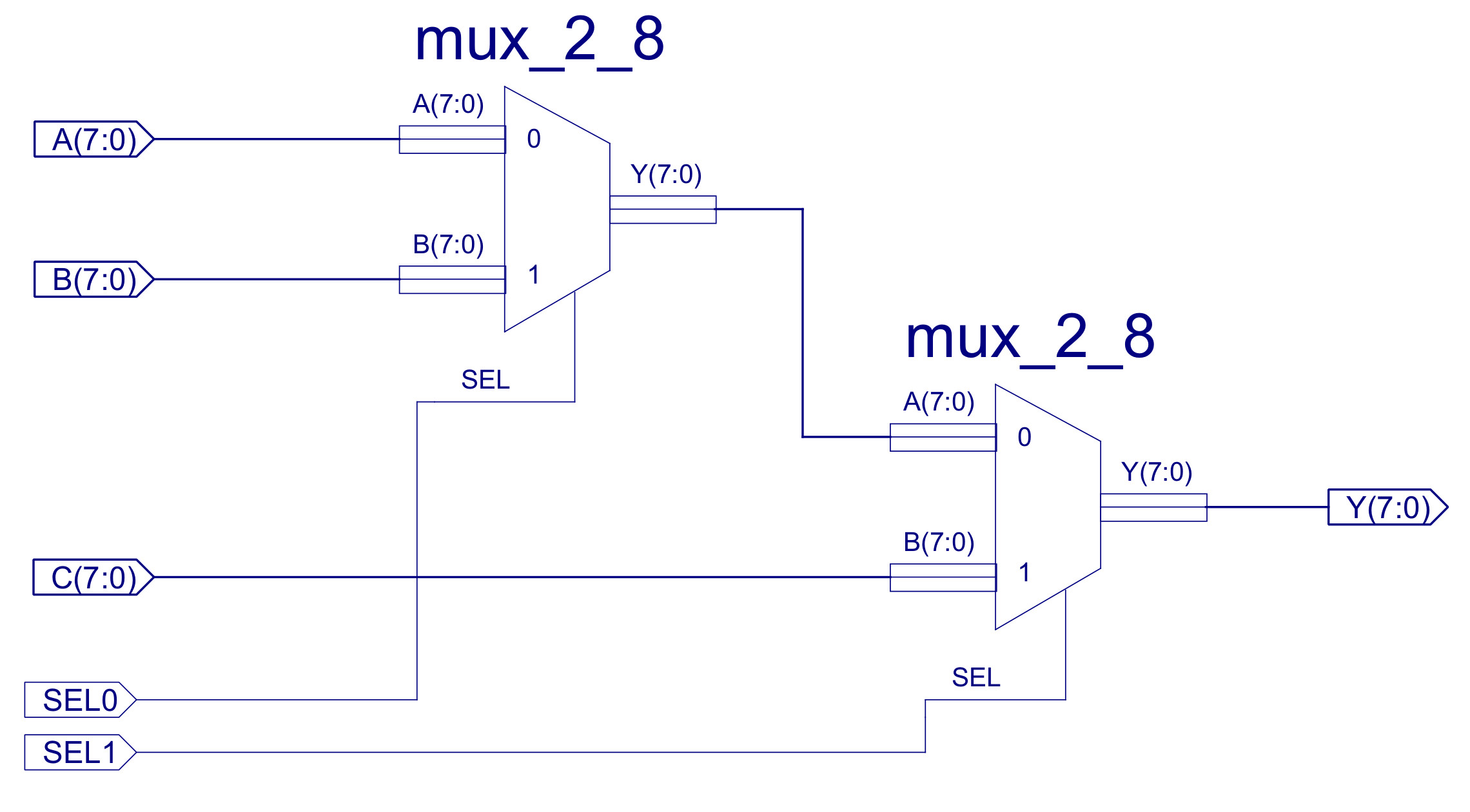
Figure 33 : MUX_3_8 circuit diagram
A simulation of the ALU performing a series of different instructions is shown in figure 34. From this you can see that operands are sent to the ALU during the decode phase and results written to the ACC in the execution phase.
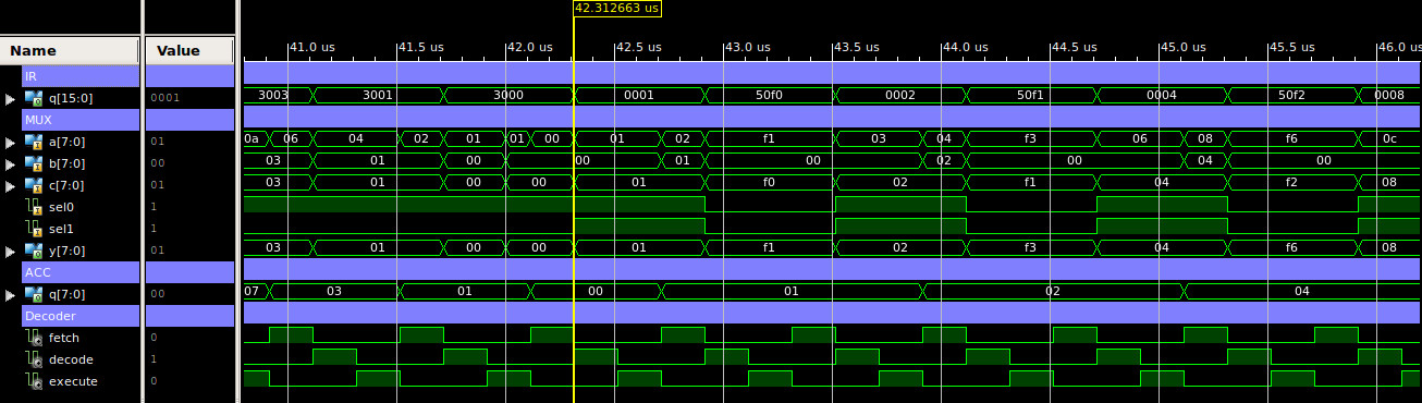
Figure 34 : ALU timing diagram
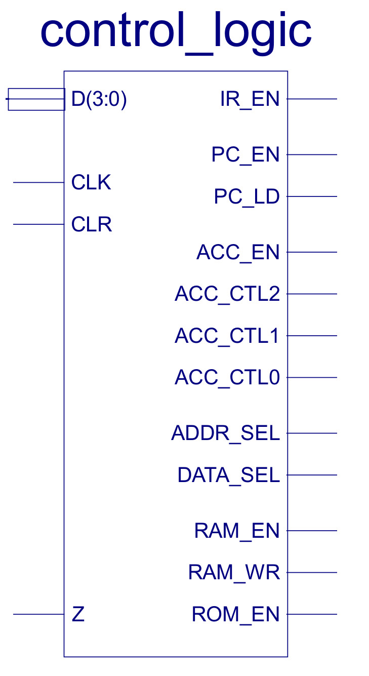
Figure 35 : Decoder
Originally this control logic was going to be a direct copy (with perhaps a few small mods) of the decoder circuit used in the bread-board version of this processor, for more information on the original design refer to the previous documentation: (Link). However, the SPLD and FPGA have different hardware architectures, resulting in different design decisions when it comes to implementation. Therefore, i decided to re-jig the control logic to better match the FPGA's internals. The two main changes are that the FPGA uses uni-directional data buses i.e. no tri-state drivers, we also have lots of spare hardware resources in the FPGA, so i did not need to go for a bit-sliced ALU. Both of these changes allow logic simplifications. Also, i had one eye on the final demo for this CPU and how this processor would be used in labs, so i decided to add a new ADDM instruction. Again, to simplify hardware construction this version of the processor only has a very limited instruction set, supporting 10 different instructions and two addressing modes, as shown below (assembly : machine-code).
In this instruction syntax X=Not-used, K=Constant and A=Address, supporting immediate and absolute addressing modes. The RTL description of these instructions are:
Note, in RTL syntax "<-" reads as "updated with", M[X] is memory, addressed at location X.
The control signals (micro-instructions) needed to implement these RTL descriptions are shown in figure 36. The biggest changes are to the ALU control signals, owing to the move away from a bit-sliced implementation, simplifying logic. Also, the DATA_SEL line was re-purposed. In the bread-board implementation this signal was used to control the bi-directional data bus. As this was no longer required, it is used to control the ALU's data multiplexer, again allowing a reduction in the required number of logic gates.
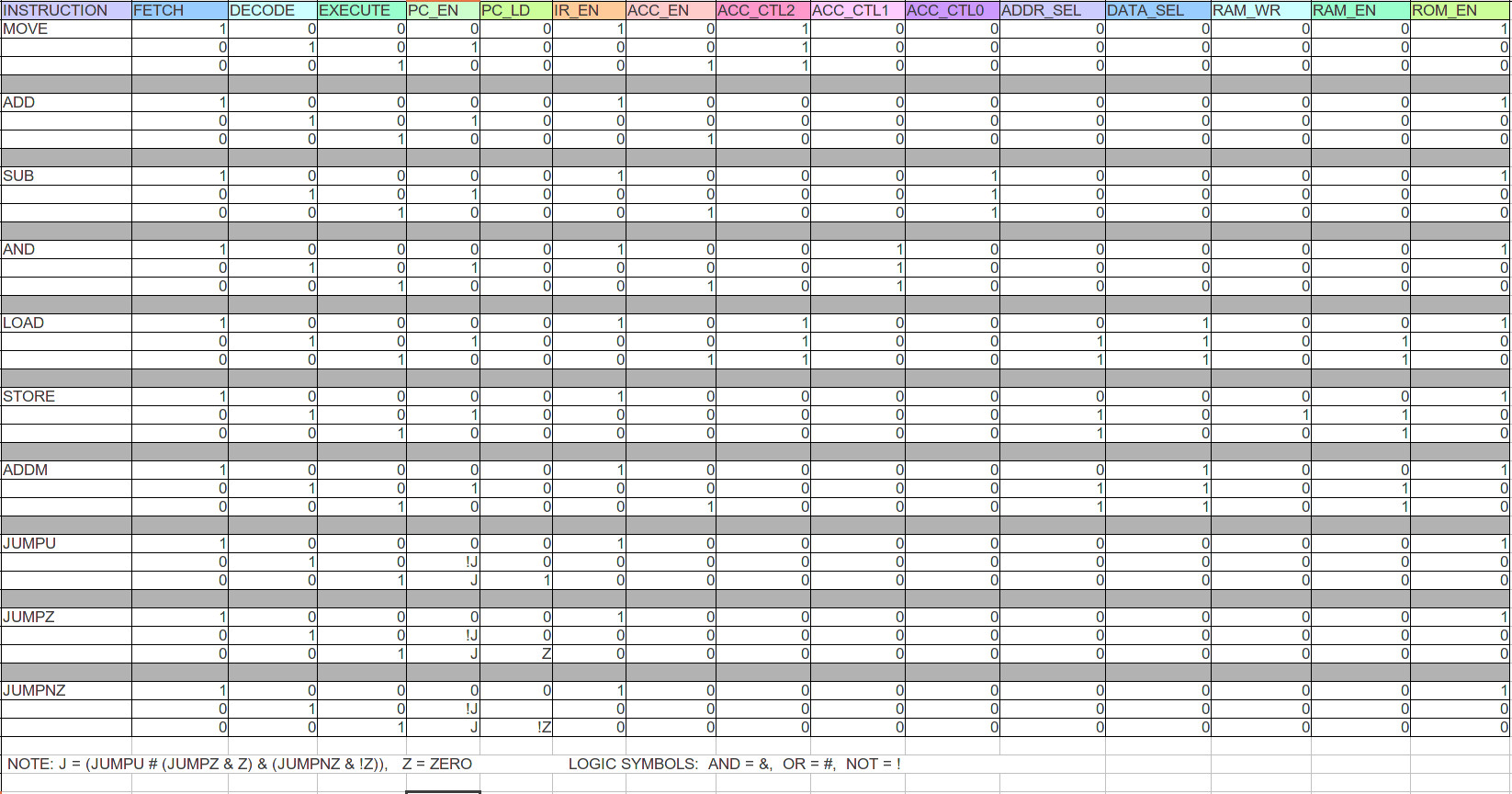
Figure 36 : micro_instructions
From this truth table the following Boolean equations can be derived (expressed in CUPL syntax) :
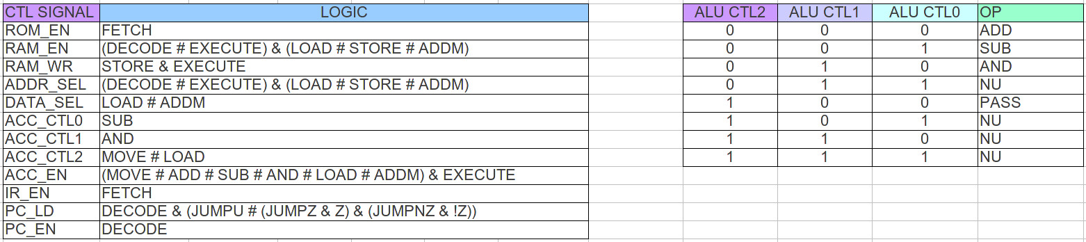
Figure 37 : control logic
The implementation of these equations, component CONTROL_LOGIC is shown in figure 38.
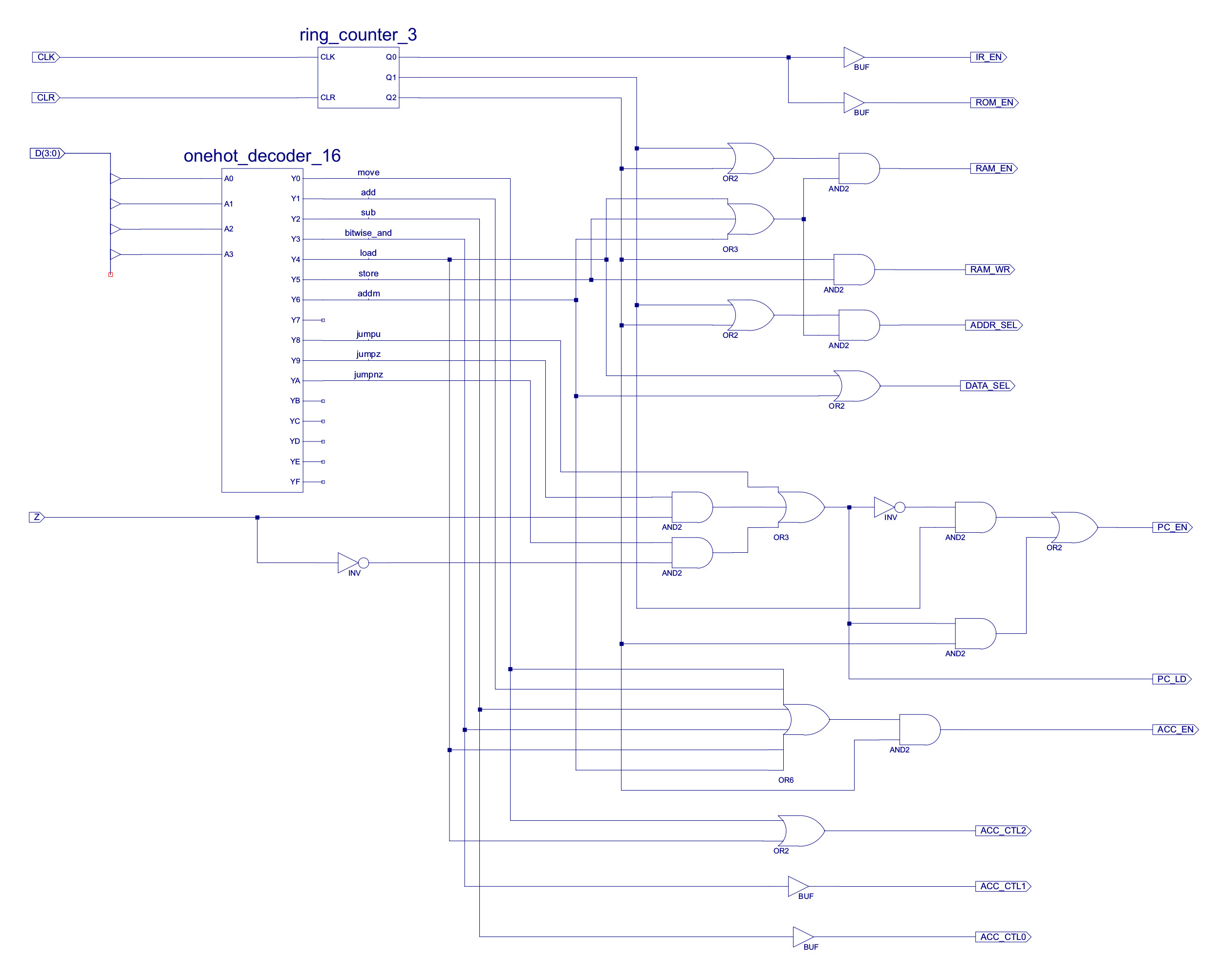
Figure 38 : Control logic decoder circuit diagram
The top nibble (4bits) of the IR contains each instruction's opcode, this drives a 4-to-16 one-hot decoder, as shown in figure 39, who's outputs are used to identify which instruction is to be executed. The current state of the processor is represented by a 3bit ring counter as shown in figure 40. The outputs from these two components are then combined using the appropriate logic gates to generate the control signals needed to implement the required functionality of each instruction.
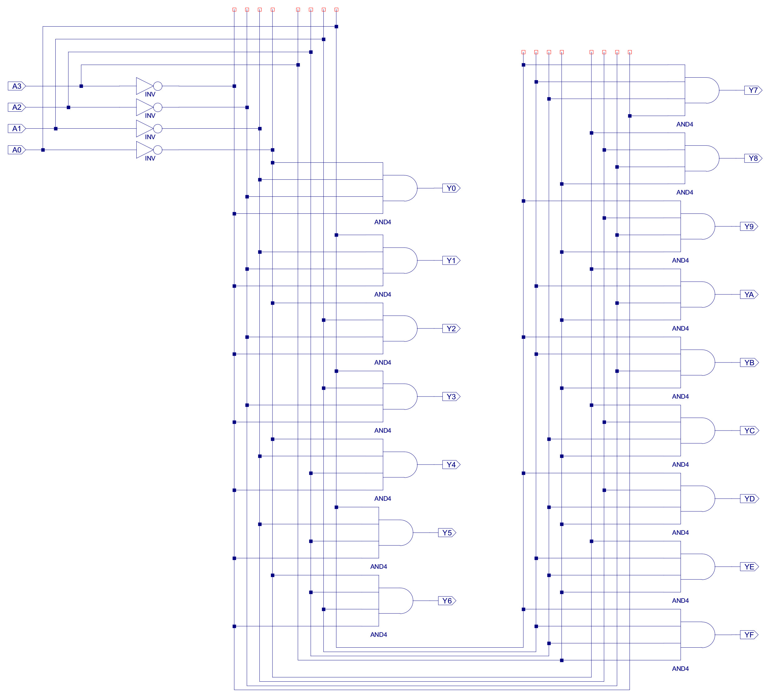
Figure 39 : one-hot decoder circuit diagram
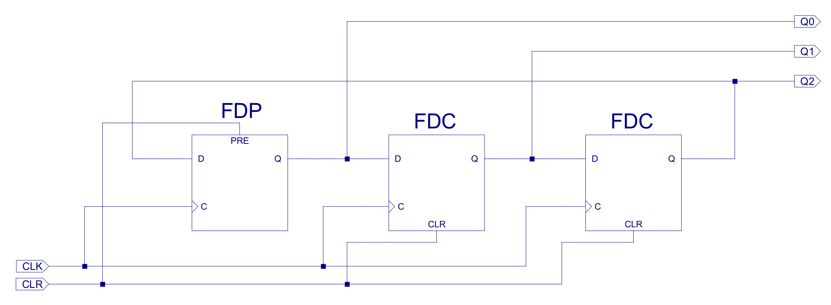
Figure 40 : ring counter circuit diagram
For initial testing i only need to create a simulation model, to ensure that each instruction is executed correctly i.e. at this stage don't need to test in the FPGA. Therefore, we can use a high level simulation model for the processor's memory. The main advantage of this is that its easy to configure i.e. to load the required instructions and data. These values are generated by the previously described assembler, slightly modified to generate a .dat file that could be loaded into this memory. The loadable VHDL memory model is shown below:
=============================================================================================================
-- *
-- * Copyright (c) Mike
-- *
-- * File Name: ram_256x16_sim.vhd
-- *
-- * Version: V1.0
-- *
-- * Release Date:
-- *
-- * Author(s): M.Freeman + others
-- *
-- * Description: simulation memory model
-- *
-- * Conditions of Use: THIS CODE IS COPYRIGHT AND IS SUPPLIED "AS IS" WITHOUT WARRANTY OF ANY KIND, INCLUDING,
-- *                    BUT NOT LIMITED TO, ANY IMPLIED WARRANTY OF MERCHANTABILITY AND FITNESS FOR A
-- *                    PARTICULAR PURPOSE.
-- *
-- * Notes: wrote this a while back, a blending of other designs, sorry lost original sources
-- *
-- =============================================================================================================

use std.textio.all;

Library IEEE;
use IEEE.std_logic_1164.all;
use IEEE.std_logic_unsigned.all;
use IEEE.std_logic_arith.all;

entity ram_256x16_sim is
  generic (
    load_file_name     : string := "ram.dat";
    load_file_name_mem : string := "ram.mem";
    load_file_name_coe : string := "ram.coe";
    dump_file_name_coe : string := "dump.coe" );
  port (
    CLK      : in  std_logic;
    ADDR_IN  : in  std_logic_vector( 7 downto 0 );
    DATA_IN  : in  std_logic_vector( 15 downto 0 );
    DATA_OUT : out std_logic_vector( 15 downto 0 );
    EN       : in  std_logic;
    WE       : in  std_logic;
    DUMP     : in  std_logic
  );
end ram_256x16_sim;

architecture ram_256x16_sim_arch of ram_256x16_sim is
begin

  mem: process
    subtype word is std_logic_vector( 15 downto 0 );
    type mem_array is array (natural range 255 downto 0) of word;

    variable mem: mem_array;
    variable address : natural;
    variable L : line;

	 variable saved : boolean := False;

     --
     -- CONVERT NIBBLE TO CHAR
     --
    function hex_to_char (nibble: std_logic_vector(3 downto 0)) return character is
      variable hex: character;
    begin
      case nibble is
        when "0000" => hex := '0';
        when "0001" => hex := '1';
        when "0010" => hex := '2';
        when "0011" => hex := '3';
        when "0100" => hex := '4';
        when "0101" => hex := '5';
        when "0110" => hex := '6';
        when "0111" => hex := '7';
        when "1000" => hex := '8';
        when "1001" => hex := '9';
        when "1010" => hex := 'A';
        when "1011" => hex := 'B';
        when "1100" => hex := 'C';
        when "1101" => hex := 'D';
        when "1110" => hex := 'E';
        when "1111" => hex := 'F';
        when others => hex := 'X';
      end case;
      return hex;
    end hex_to_char;

    --
    -- LOAD MEM
    --
    procedure load( mem: inout mem_array) is

      file load_data_file : text open READ_MODE  is load_file_name;
      file mem_data_file  : text open WRITE_MODE is load_file_name_mem;
      file coe_data_file  : text open WRITE_MODE is load_file_name_coe;

      variable data_string : line;
      variable mem_string : line;
      variable coe_string : line;

      variable addr, data, count : natural;
      variable data_char : character;
      variable valid : boolean;

      variable bin_addr : std_logic_vector(7 downto 0);
      variable bin_data : std_logic_vector(15 downto 0);

    begin
      write( output, "ram initialization" );

      for addr in 0 to 255
      loop
        mem( addr ) := "0000000000000000";
      end loop;

      while not endfile( load_data_file )
      loop
        readline( load_data_file, data_string );
        read( data_string, addr, valid);        -- address

        if (valid)
        then
          read( data_string, data_char );   -- space

          data := 0;
          count := 0;

          while count < 16
          loop
            read( data_string, data_char );
            if data_char /= ' '
            then
              count := count + 1;     -- count bits processed
              data := data + data;    -- shift string
              if data_char = '1'
              then
                data :=data + 1;      -- insert 1 if set
              end if;
            end if;
          end loop;

          write( data_string , addr);
          write( data_string, ' ' );
          write( data_string, data);
          writeline( output, data_string );
          mem( addr ) := conv_std_logic_vector( data, 16 );

          bin_addr := (conv_std_logic_vector( (addr*3), 8));
	  write( mem_string, '@');
          write( mem_string , hex_to_char( bin_addr(7 downto 4) ) );
          write( mem_string , hex_to_char( bin_addr(3 downto 0) ) );

          bin_data := conv_std_logic_vector( data, 16);
          write( mem_string , ' ');
          write( mem_string , hex_to_char( bin_data(3 downto 0) ) );
          write( mem_string , hex_to_char( bin_data(7 downto 4) ) );
          write( mem_string , hex_to_char( bin_data(11 downto 8) ) );
          write( mem_string , hex_to_char( bin_data(15 downto 12) ) );
	  writeline( mem_data_file, mem_string );
        end if;
      end loop;

      write( coe_string , "memory_initialization_radix = 16;");
      writeline( coe_data_file, coe_string );
      write( coe_string , "memory_initialization_vector = ");
      writeline( coe_data_file, coe_string );

      for addr in 0 to 255
      loop
        bin_data :=  mem( addr );
        write( coe_string , ' ');
        write( coe_string , hex_to_char( bin_data(15 downto 12) ) );
        write( coe_string , hex_to_char( bin_data(11 downto 8) ) );
        write( coe_string , hex_to_char( bin_data(7 downto 4) ) );
        write( coe_string , hex_to_char( bin_data(3 downto 0) ) );
        if addr = 255
	then
	  write( coe_string , " ;" );
	else
          write( coe_string , " ," );
        end if;
        writeline( coe_data_file, coe_string );

      end loop;
    end load;

    --
    -- SAVE MEM
    --
    procedure save( mem: inout mem_array) is
      file coe_data_file  : text open WRITE_MODE is dump_file_name_coe;

      variable coe_string : line;
      variable addr : natural;
      variable bin_data : std_logic_vector(15 downto 0);

    begin
      write( coe_string , "memory_initialization_radix = 16;");
      writeline( coe_data_file, coe_string );
      write( coe_string , "memory_initialization_vector = ");
      writeline( coe_data_file, coe_string );

      for addr in 0 to 255
      loop
        bin_data :=  mem( addr );
        write( coe_string , ' ');
        write( coe_string , hex_to_char( bin_data(15 downto 12) ) );
        write( coe_string , hex_to_char( bin_data(11 downto 8) ) );
        write( coe_string , hex_to_char( bin_data(7 downto 4) ) );
        write( coe_string , hex_to_char( bin_data(3 downto 0) ) );
	if addr = 255
	then
	  write( coe_string , " ;" );
	else
          write( coe_string , " ," );
        end if;
	writeline( coe_data_file, coe_string );

      end loop;
    end save;

  --
  -- MAIN LOOP
  --
  begin
    load( mem );
    loop
      if (EN = '1')
      then
        address := conv_integer( ADDR_IN );
        if (WE = '1')
        then
          mem( address ) := DATA_IN;
        end if;
	     DATA_OUT <= mem( address );
      end if;

      if (DUMP = '1' and not saved)
      then
        save( mem );
        saved := True;
      end if;
      wait on clk;

    end loop;
  end process;

end ram_256x16_sim_arch;
The VHDL source file is available here (Link). To test this implementation of the processor the following test code: (Link), is used. This producing the following machine code file: (Link), which is passed to the simulation memory model as a generic parameter i.e. loaded at the start of the simulation. The code also generates a .coe and .mem memory files that can be used to initialise an IP-Core memory component that can be used on the FPGA. A simulation of this processor executing this code is show in figure 41. A blur of squiggles, but you can see the opcode value changing on the decoder D input and their associated control signal updates.
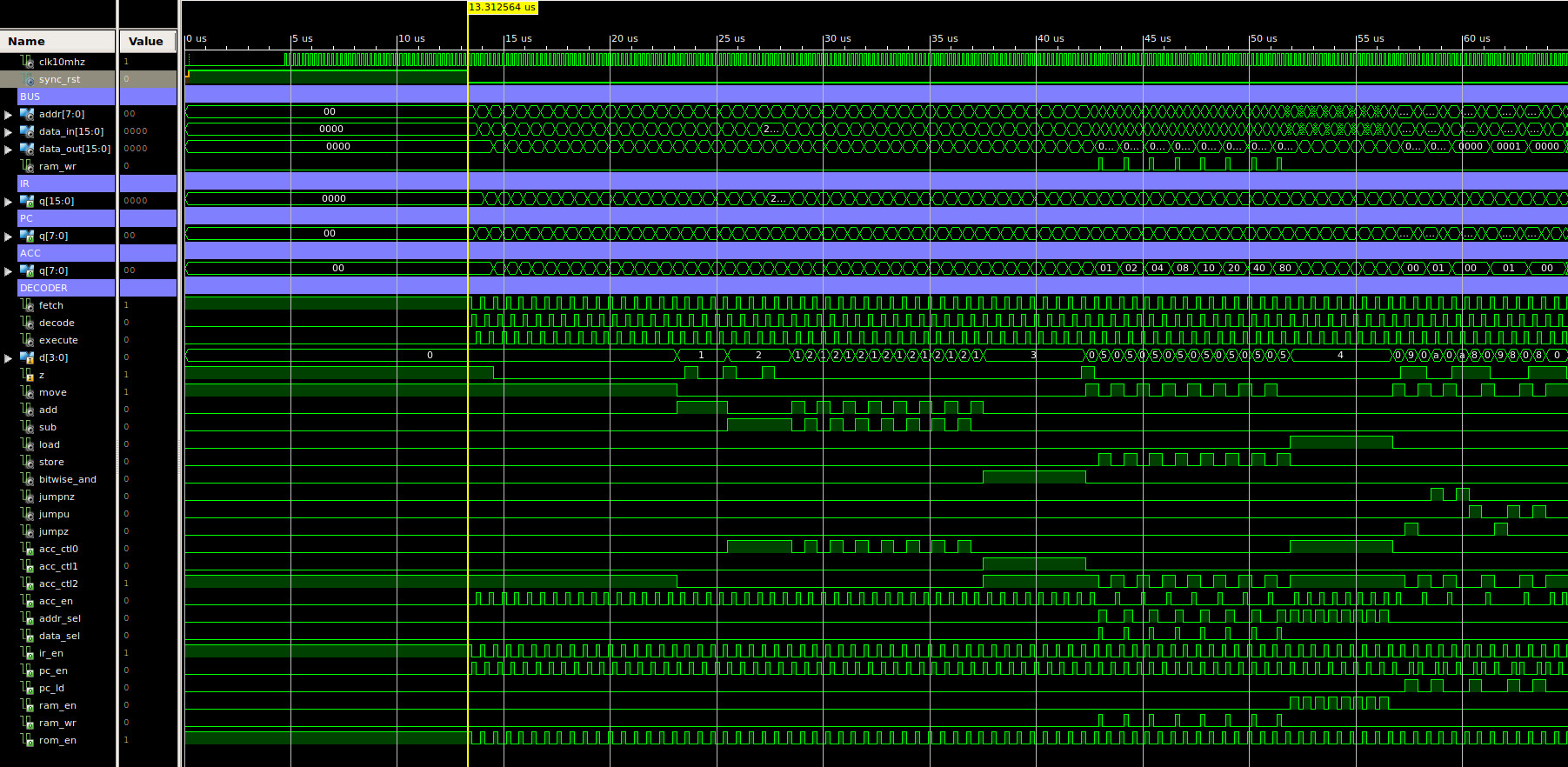
Figure 41 : test code timing diagram
All seems fine, nothing major needed fixing. With the basic design tested now need to test on the FPGA.
The previous simulation model can not be synthesised i.e. implemented on an FPGA. Therefore, to actually run the processor on the FPGA we have to use the FPGA's memory devices i.e. BlockRAMs. These can either be instantiated through the IP-Core wizards or from the standard component library (this will vary with FPGA). To test if these designs worked on the FPGA you need something that will generate an output signal i.e. once you have uploaded the .bit file onto the FPGA its difficult to "see" what is actually happening in the FPGA. Initial testing was on the Z7 ZYBO board. This has 4 LEDS and an RGB LED, so i decided to go back to the favoured Christmas lights demo.
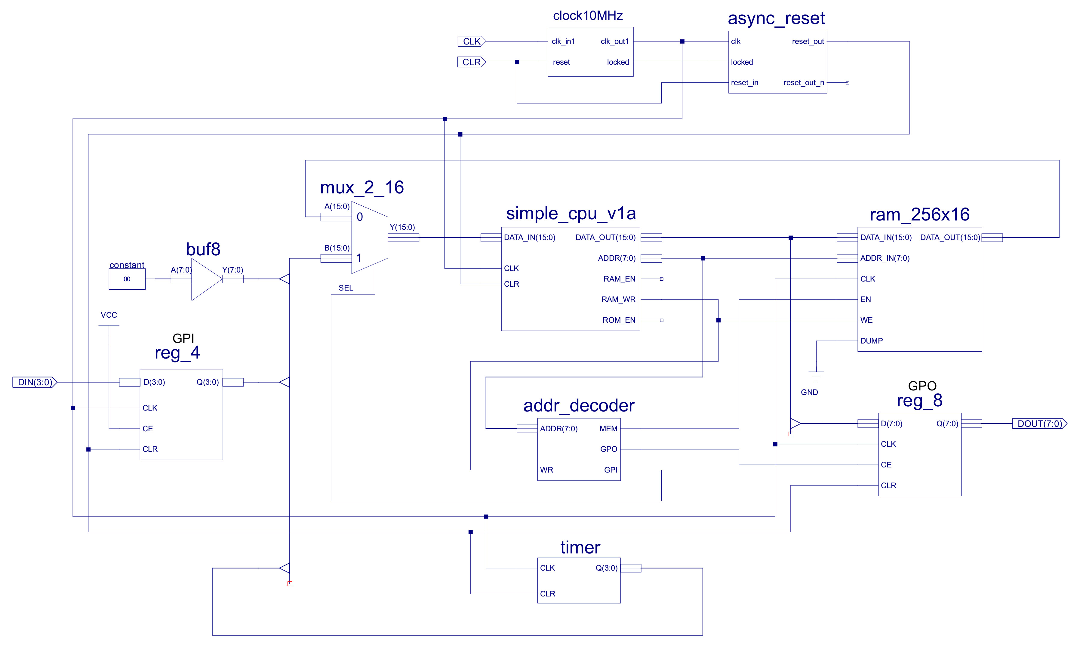
Figure 42 : GPIO
The simple CPU GPIO ISE project files for this computer can be downloaded here: (Link).
To interface the LEDs and switches to the CPU i added an 8bit general purpose input (GPI) and an 8bit general purpose output (GPO). These devices are mapped into the processor's address space, assigned the memory address 0xFF. From each memory transaction the address decoder component ADDR_DECODER is used to determine which device should have access to the system's buses i.e. Memroy, Output-port or Input-port. This component monitors the processor's address and control buses, controlling the enable signals: MEM, GPI and GPO. The hardware used to produce these signals is shown in figure 43.
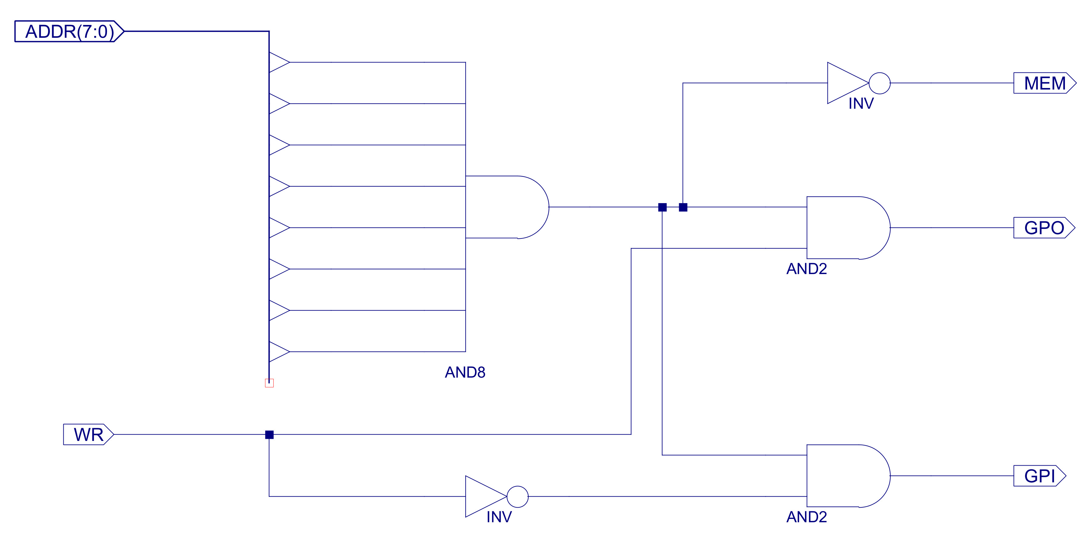
Figure 43 : Address decoder
The address bus is passed to an 8bit AND gate. If all address lines are logic '1' i.e. address 0xFF, this AND gate will produce a logic 1, enabling the two two-input AND gates which control the GPO and GPI enable lines. If the RAM_WR enable signal (WR) is high the GPO line is enabled. If the RAM_WR enable signal (WR) is low the GPI line is enabled i.e. the same address (0xFF) is used for both input and output port. If any address other than 0xFF is used the MEM line is enabled, allowing the processor to read or write to the RAM.
The GPI control line is used to control the data multiplexer MUX_2_16, selecting either the GPI input data or data from the RAM. When selecting input data the lower 4bits are sourced from an input register. This register is updated on each clock cycle, the lower four D inputs are connected to the four external switches. Note, the reason for using the 4bit register components is to remove setup-and-hold timing problems associated with asynchronous inputs i.e. the switches can changed independent of the clock. Therefore, to ensure that there are no race hazards in the processor all external input signals are registered, synchronising them to the system clock. The high 4bits of the input data is connected to the timer component. As the first demo is a lights display, signals will need to be updated every second or so. These delays could be implemented in software, but to simplify this task the counters in the timer component shown in figure 45 are used.
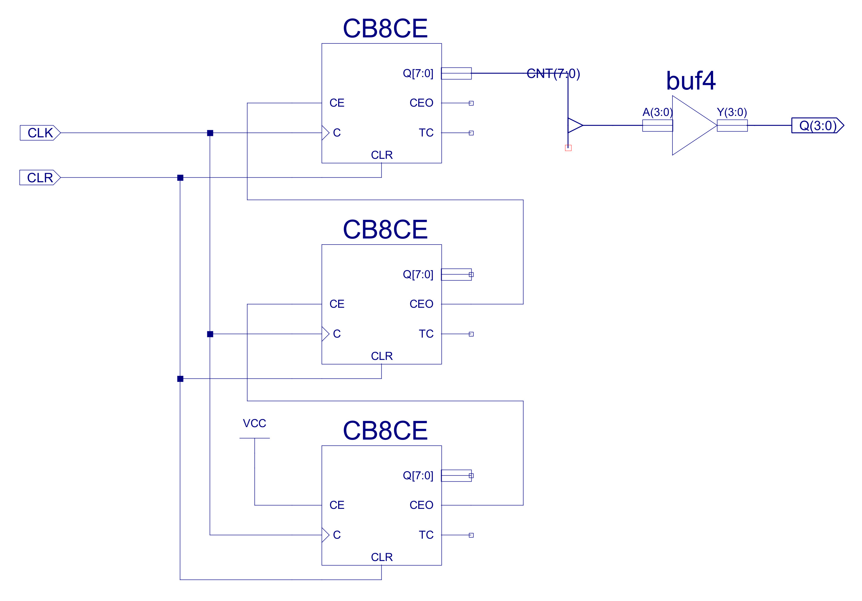
Figure 44 : timer
This component uses three eight bit binary counters: CB8CE, sourced from the standard Xilinx library. These counters are cascaded together to produce a 24bit counter, the top 4bits being connected to the general purpose input port. The max count value of the counter is 16777216, with a 10MHz clock this signal will change every 1.6 seconds.
The GPO output port is simply an 8bit register, when the processor writes a data value to address 0xFF, the CE line is enabled and the lower 8bits of the this bus are stored in this register, its Q outputs are connected to the LEDs, as shown below:
A simple test program to flash the LEDs on and off every second-ish is shown below:
#
# GPIO TEST PROGRAM
#

000 move    0xFF  -- set all bits in ACC to 1
001 store   0xFF  -- store ACC to output port

002 load    0xFF  -- read input port
003 and     0x80  -- mask out MSB i.e. timer Q3
004 jumpz   2     -- if 0 jump back to 2 and repeat

005 move    0     -- set all bits in ACC to 0
006 store   0xFF  -- store ACC to output port

007 load    0xFF  -- read input port
008 and     0x80  -- mask out MSB i.e. timer Q3
009 jumpnz  7     -- if 1 jump back to 7 and repeat

010 jump    0     -- repeat loop, jump back to 0
Note, an LED is illuminated when a logic 1 is set on the appropriate output. This assembly language program is converted into the BlockRAM configuration file: ram.mem (below), using the simpleCPUv1a_as.py assembler. Data is byte addressable i.e. each 16bit data value is aligned on an even memory address.
@0000 FF00
@0002 FF05
@0004 FF04
@0006 0803
@0008 2009
@000A 0000
@000C FF05
@000E FF04
@0010 0803
@0012 700A
@0014 0008
Figure 45 : ram.mem - BlockRAM configuration file
A synthesizable memory model is constructed from four RAMB16_S4 BlockRAM components to produce a 4K x 16bit memory device. This is a lot larger than the required 256 x 16bit memory used by the simpleCPUv1a processor, however, i kept this design structure as its used in the later simpleCPU implementations/versions i.e. allows re-use of scripts and components etc. It also makes debugging simpler as it allows you to easily read the BlockRAM files i.e. each memory stores a nibble (4bits) of each 16bit instruction. The RAMB16_S4 BlockRAM memory components are defined in the file: blockram_4Kx4.vhd, a wrapper component, shown in figure 47. Note "..." indicates where lines have been removed to save space.
-- =============================================================================================================
-- *
-- * Copyright (c) Mike
-- *
-- * File Name: blockram_4Kx4.vhd
-- *
-- * Version: V1.0
-- *
-- * Release Date:
-- *
-- * Author(s): M.Freeman
-- *
-- * Description: Random Access Memory single port module
-- *
-- * Conditions of Use: THIS CODE IS COPYRIGHT AND IS SUPPLIED "AS IS" WITHOUT WARRANTY OF ANY KIND, INCLUDING,
-- *                    BUT NOT LIMITED TO, ANY IMPLIED WARRANTY OF MERCHANTABILITY AND FITNESS FOR A
-- *                    PARTICULAR PURPOSE.
-- *
-- =============================================================================================================

LIBRARY IEEE;
USE IEEE.STD_LOGIC_1164.ALL;
USE IEEE.STD_LOGIC_ARITH.ALL;
USE IEEE.STD_LOGIC_UNSIGNED.ALL;

LIBRARY UNISIM;
USE UNISIM.vcomponents.ALL;

ENTITY blockram_4Kx4 IS
GENERIC (
  INIT_00 : bit_vector := X"0000000000000000000000000000000000000000000000000000000000000000";
  ...
  INIT_3F : bit_vector := X"0000000000000000000000000000000000000000000000000000000000000000" );
PORT (
  clk      : IN STD_LOGIC;
  en       : IN STD_LOGIC;
  we       : IN STD_LOGIC;
  addr     : IN STD_LOGIC_VECTOR(11 DOWNTO 0);
  data_in  : IN STD_LOGIC_VECTOR(3 DOWNTO 0);
  data_out : OUT STD_LOGIC_VECTOR(3 DOWNTO 0) );
END blockram_4Kx4;


ARCHITECTURE blockram_4Kx4_arch OF blockram_4Kx4 IS

  component RAMB16_S4
  generic (
     INIT : bit_vector := X"0";
     INIT_00 : bit_vector := X"0000000000000000000000000000000000000000000000000000000000000000";
     ...
     INIT_3F : bit_vector := X"0000000000000000000000000000000000000000000000000000000000000000";
     SRVAL : bit_vector := X"0";
     WRITE_MODE : string := "WRITE_FIRST" );
  port (
     DO : out STD_LOGIC_VECTOR (3 downto 0);
     ADDR : in STD_LOGIC_VECTOR (11 downto 0);
     CLK : in STD_ULOGIC;
     DI : in STD_LOGIC_VECTOR (3 downto 0);
     EN : in STD_ULOGIC;
     SSR : in STD_ULOGIC;
     WE : in STD_ULOGIC );
  end component;

  attribute BOX_TYPE of
  RAMB16_S4 : component is "PRIMITIVE";

BEGIN

  ram_module : RAMB16_S4
  GENERIC MAP(
    INIT_00 => INIT_00,
    ...
    INIT_3F => INIT_3F )
  PORT MAP(
      DO => data_out,
      di => data_in,
      addr => addr,
      clk => clk,
      en => en,
      ssr => '0',
      we => we );

END blockram_4Kx4_arch;
Figure 46 : 4Bit memory - blockram_4Kx4.vhd
Four of these components are instantiated in the ram_256x16_syn.vhd component, the high nibble of the 12bit address is zeroed to give the required eight bit address used by the simpleCPU, as shown in figure 47.
-- =============================================================================================================
-- *
-- * Copyright (c) Mike
-- *
-- * File Name: ram_256x16_syn.vhd
-- *
-- * Version: V1.0
-- *
-- * Release Date:
-- *
-- * Author(s): M.Freeman
-- *
-- * Description: synthesis memory model
-- *
-- * Conditions of Use: THIS CODE IS COPYRIGHT AND IS SUPPLIED "AS IS" WITHOUT WARRANTY OF ANY KIND, INCLUDING,
-- *                    BUT NOT LIMITED TO, ANY IMPLIED WARRANTY OF MERCHANTABILITY AND FITNESS FOR A
-- *                    PARTICULAR PURPOSE.
-- *
-- * Notes:
-- *
-- =============================================================================================================

library IEEE;
use IEEE.STD_LOGIC_1164.ALL;

library work;
use work.memory_pkg_mem.all;

entity ram_256x16 is
  port (
    CLK      : in  std_logic;
    ADDR_IN  : in  std_logic_vector( 7 downto 0 );
    DATA_IN  : in  std_logic_vector( 15 downto 0 );
    DATA_OUT : out std_logic_vector( 15 downto 0 );
    EN       : in  std_logic;
    WE       : in  std_logic;
    DUMP     : in  std_logic
  );
end ram_256x16;


architecture ram_256x16_arch of ram_256x16 is

  COMPONENT blockram_4Kx4
  GENERIC (
    INIT_00 : bit_vector := X"0000000000000000000000000000000000000000000000000000000000000000";
    ...
    INIT_3F : bit_vector := X"0000000000000000000000000000000000000000000000000000000000000000" );
  PORT (
    clk : IN STD_LOGIC;
    en : IN STD_LOGIC;
    we : IN STD_LOGIC;
    addr : IN STD_LOGIC_VECTOR(11 DOWNTO 0);
    data_in : IN STD_LOGIC_VECTOR(3 DOWNTO 0);
    data_out : OUT STD_LOGIC_VECTOR(3 DOWNTO 0) );
  END COMPONENT;

  SIGNAL clk_n : STD_LOGIC;
  SIGNAL addr  : STD_LOGIC_VECTOR(11 DOWNTO 0);

begin

  clk_n<= not CLK;
  addr <= "0000" & ADDR_IN;

  mem_A : blockram_4Kx4
  GENERIC MAP (
    INIT_00 => computer_MEMORY_mem_A_ram_module_INIT_00,
    ...
    INIT_3F => computer_MEMORY_mem_A_ram_module_INIT_3F )
  PORT MAP (
    clk => clk_n,
    en => EN,
    we => WE,
    addr => addr,
    data_in => DATA_IN(3 DOWNTO 0),
    data_out => DATA_OUT(3 DOWNTO 0) );

  mem_B : blockram_4Kx4
  GENERIC MAP (
    INIT_00 => computer_MEMORY_mem_B_ram_module_INIT_00,
    ...
    INIT_3F => computer_MEMORY_mem_B_ram_module_INIT_3F )
  PORT MAP (
    clk => clk_n,
    en => EN,
    we => WE,
    addr => addr,
    data_in => DATA_IN(7 DOWNTO 4),
    data_out => DATA_OUT(7 DOWNTO 4) );

  mem_C : blockram_4Kx4
  GENERIC MAP (
    INIT_00 => computer_MEMORY_mem_C_ram_module_INIT_00,
    ...
    INIT_3F => computer_MEMORY_mem_C_ram_module_INIT_3F )
  PORT MAP (
    clk => clk_n,
    en => EN,
    we => WE,
    addr => addr,
    data_in => DATA_IN(11 DOWNTO 8),
    data_out => DATA_OUT(11 DOWNTO 8) );

  mem_D : blockram_4Kx4
  GENERIC MAP (
    INIT_00 => computer_MEMORY_mem_D_ram_module_INIT_00,
    ...
    INIT_3F => computer_MEMORY_mem_D_ram_module_INIT_3F )
  PORT MAP (
    clk => clk_n,
    en => EN,
    we => WE,
    addr => addr,
    data_in => DATA_IN(15 DOWNTO 12),
    data_out => DATA_OUT(15 DOWNTO 12) );

end ram_256x16_arch;
Figure 47 : 256 x 16Bit memory - ram_256x16.vhd
The contents of these memory components are configured from the file memory.vhd, which stores the generic parameters for each memory e.g. computer_MEMORY_mem_A_ram_module_INIT_00. This data is generated by the Xilinx tool data2mem, using the files: ram.mem shown in figure 45 and mem.bmm shown in figure 48 below.
ADDRESS_SPACE mem RAMB16 [0x00000000:0x00001FFF]
  BUS_BLOCK
    computer/MEMORY/mem_A/ram_module [  3:0] LOC = X2Y20;
    computer/MEMORY/mem_B/ram_module [  7:4] LOC = X2Y21;
    computer/MEMORY/mem_C/ram_module [ 11:8] LOC = X2Y22;
    computer/MEMORY/mem_D/ram_module [15:12] LOC = X2Y23;
  END_BUS_BLOCK;
END_ADDRESS_SPACE;
Figure 48 : memory configuration file
The script to generate the BlockRAM initialisation file is:
#!/bin/sh
data2mem -bm mem.bmm -bd ram.mem -o uvh memory.vhd
which produces the following VHDL package file - memory.vhd:
-- VHDL initialization records.
--
-- Release 14.6 - Data2MEM P_INT.20160526, build 3.0.10 Apr 3, 2013
-- Copyright (c) 1995-2019 Xilinx, Inc.  All rights reserved.
--
-- Command: data2mem -bm mem.bmm -bd ram.mem -o uvh memory.vhd
--
-- Created on Monday August 19, 2019 - 07:52:45 pm, from:
--
--     Map file     - mem.bmm
--     Data file(s) - ram.mem
--
-- Address space 'mem' [0x00000000:0x00001FFF], 8192 bytes in size.
--
-- Bus width = 16 bits, number of bus blocks = 1.

library ieee;
use ieee.std_logic_1164;

package memory_pkg_mem is

-- BRAM 0 in address space [0x00000000:0x00001FFF], bit lane [3:0]
-- INST computer/MEMORY/mem_A/ram_module LOC = RAMB16_X2Y20;
	constant computer_MEMORY_mem_A_ram_module_INIT_00  : bit_vector(0 to 255) := x"00000000000000000000000000000000000000000000000000000070FF020FFF";

-- BRAM 1 in address space [0x00000000:0x00001FFF], bit lane [7:4]
-- INST computer/MEMORY/mem_B/ram_module LOC = RAMB16_X2Y21;
	constant computer_MEMORY_mem_B_ram_module_INIT_00  : bit_vector(0 to 255) := x"00000000000000000000000000000000000000000000000000000008FF008FFF";

-- BRAM 2 in address space [0x00000000:0x00001FFF], bit lane [11:8]
-- INST computer/MEMORY/mem_C/ram_module LOC = RAMB16_X2Y22;
	constant computer_MEMORY_mem_C_ram_module_INIT_00  : bit_vector(0 to 255) := x"0000000000000000000000000000000000000000000000000000000000000000";

-- BRAM 3 in address space [0x00000000:0x00001FFF], bit lane [15:12]
-- INST computer/MEMORY/mem_D/ram_module LOC = RAMB16_X2Y23;
	constant computer_MEMORY_mem_D_ram_module_INIT_00  : bit_vector(0 to 255) := x"000000000000000000000000000000000000000000000000000008A345093450";

end memory_pkg_mem;
If you compare this to figure 45, you can match the instruction nibbles stored in each memory location. Alternatively, the BlockRAMs within the pre-compiled .bit file used to configure the FPGA can be directly updated using the script below:
#!/bin/sh
data2mem -bm mem.bmm -bd ram.mem -bt computer.bit -o b updated_computer.bit
This removes the need to re-synthesise the design, speeding up code development. A short video of the FPGA board running this code is available here: (Link).
Additional instructions can be created without modifying the hardware by combining existing instructions within a macro. These can then be used to create different light displays
The simplest addition to the processor's instruction set are instructions that set the ACC to a new value e.g. CLR or SET. The required macros are shown below:
define( clr,`move 0x00')
define( set,`move 0xFF')
Shift instructions are normally implemented using a barrel shifter (Link). Each shift to the right is the same as performing a multiplication by two, consider the value 0x0A, decimal 10, each time it is multiplied by 2 the bit pattern (1010) is shifted to the right one position:
0x0A = 10 = 00001010     mul 2     00010100 = 20
                         mul 2     00101000 = 40
                         mul 2     01010000 = 80
                         mul 2     10100000 = 160
Multiplication on a CPU is normally implemented using dedicated hardware (Link), however, it can also be implemented using repeated addition e.g. 15x2 = 15+15, 15x3 = 15+15+15 etc. Note, this technique is fine for small values, but becomes impractical for larger value e.g. 15 x 255, will take a little while to process. To implement a shift right instruction the required macro is shown below:
define( sr0,`load $1
addm $1
store $1')
The bitwise-OR instructions performs the opposite function to the the bitwise-AND i.e. the bitwise-AND is used to clear bit positions, the bitwise-OR to set bit positions. To implement a bitwise-OR instruction the required macro is shown below:
define( ora,`and eval($1 ^ 255)
add $1')
Note, bitwise-AND instructions can also be implemented using the subtract instruction clearing set bit positions, an example of this is shown in the bread-baord implementations test code: (Link).
As previously discussed (Link) subroutines allow repeated code to be written once and used many times within a program. However, to do this the processor needs to keep a track of where it needs to return to after the subroutine has completed i.e. a subroutine's first address is fixed, the main program's return address will vary. Typically, this information is stored in read/write memory on a stack. This requires specialised instructions and hardware modifications to the processor. In early computers to avoid these overheads a different approach was taken i.e. self-modifying code (Link). The first computer to use subroutines i.e. a pre-written software libraries, was EDSAC (Link), implementing the subroutine mechanism using a "Wheeler jump", a technique named after its creator David Wheeler.
In a Wheeler Jump the returning JUMP in the subroutine is modified i.e. re-written, as the program is executed, so that the program returns back to the correct instruction. An example is shown is figure 49:
010  move 10     --  load ACC with the calling address
011  jump 55     --  jump to address of subroutine
012  store 0xFF  --  store result from subroutine to address 0xFF

...

020  move 20     --  load ACC with the calling address
021  jump 55     --  jump to address of subroutine
022  store 0xFF  --  store result from subroutine to address 0xFF

...
                 --  return address passed to subroutine via ACC
055  add 2       --  first address of subroutine, add 2 to generate return address
056  store 8 58  --  overwrite final instruction in subroutine, unused bits set to "1000" = 8
057  ...         --  subroutine code
058  jump 0x00   --  return JUMP instruction
059
Figure 49 : Wheeler jump example
The STORE instruction at address 56, writes the return address in the ACC to memory location 58. This would normally overwrite the opcode value, however, as bits IR(12 downto 8) are not normally used, these can be used to extend the functionality of the store instruction, allowing a 12bit value to be written to the specified memory address, as shown in figure 50.
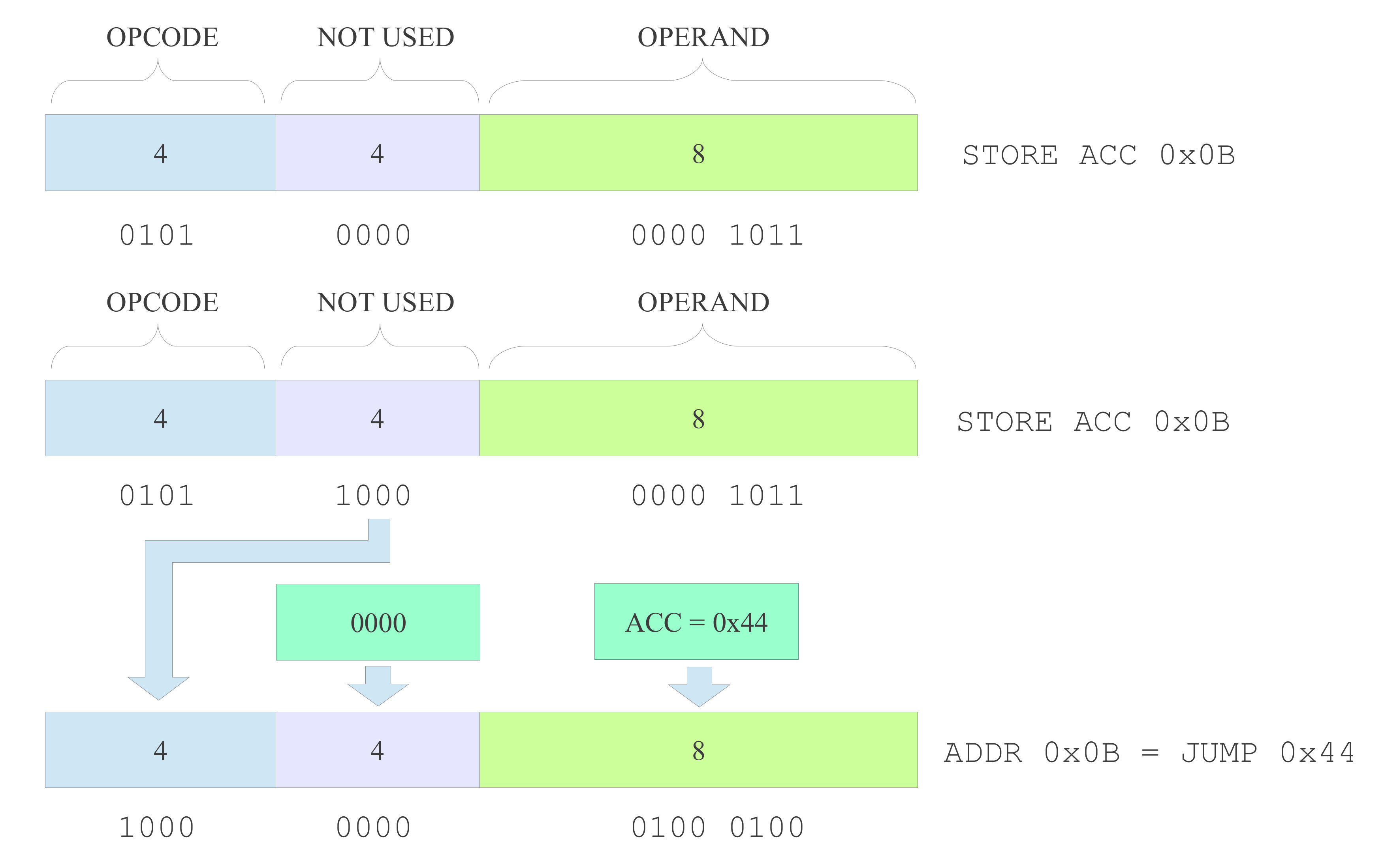
Figure 50 : instruction unused bits
This example shows that bit patterns "0101 0000 00001011" and "0101 1000 00001011" represent the same instruction STORE ACC 0x0B. Note, remember only the top nibble (4 bits) are decoded, the low nibble in the high byte is not used by the decoder (not true for later versions of this processor). However, these unused bits IR(12 downto 8) can be used to set the top nibble of the data written to address 0x0B i.e. set a new opcode field. This allows the store instruction to write the JUMP opcode in the high nibble and the ACC to the low byte i.e. the address operand, creating a new JUMP instruction e.g. JUMP 0x44 at address 0x0B. This process is performed each time the subroutine is called e.g. in figure 49 the first time the subroutine is called the instruction JUMP 12 is written to address 58, the second time the instruction JUMP 22 is written to address 58.
As shown in figure 49 the STORE instruction now takes two operands: a 4bit value form IR(12 downto 8) and an 8bit value for the normal address field. Therefore, the assembler was modified accordingly to accept a one or two operand store instruction.
To generate a different display the ADDM instruction can be used. Using this instruction a simple shift instruction can be implemented. The new software is shown below:
#
# GPIO TEST PROGRAM
#

000 move    1     -- set LSB, ACC to initial value
001 store   0xF0  -- store to tmp variable
002 store   0xFF  -- store ACC to output port

003 load    0xFF  -- read input port
004 and     0x40  -- mask out MSB i.e. timer Q3
005 jumpz   3     -- if 0 jump back to 3 and repeat

006 load    0xF0  -- read tmp variable
007 addm    0xF0  -- add tmp variable to ACC i.e. x2
008 store   0xF0  -- store to tmp variable
009 store   0xFF  -- store ACC to output port

00A load    0xFF  -- read input port
00B and     0x40  -- mask out MSB i.e. timer Q3
00C jumpnz  10    -- if 1 jump back to 10 and repeat

00D jump    3     -- repeat loop, jump back to 3
A short video of the FPGA board running this code is available here: (Link). This code was also convert to use a subroutine passed architecture, as shown below:
#
# SUBROUTINE TEST PROGRAM
#

000 move    1 -- set LSB, ACC to initial value
001 store   0xF0 -- store to tmp variable
002 store   0xFF -- store ACC to output port

003 load    0xFF -- read input port
004 and     0x40 -- mask out MSB i.e. timer Q3
005 jumpz   3 -- if 0 jump back to 3 and repeat

006 move    6 --
007 jump    15 -- jump to subroutine MULT2

008 load    0xFF -- read input port
009 and     0x40 -- mask out MSB i.e. timer Q3
010 jumpnz  8 -- if 1 jump back to 10 and repeat

011 move    11 --
012 jump    15 -- jump to subroutine MULT2

013 jumpnz  3
014 jump    0 -- repeat loop

#
# MULT 2 subroutine
#

015 add     2 -- generate return address
016 store   8 21
017 load    0xF0 -- read tmp variable
018 addm    0xF0 -- add tmp variable to ACC i.e. x2
019 store   0xF0 -- store to tmp variable
020 store   0xFF -- store ACC to output port
021 jump    0x00 --
The is converted into machine code (below) using the updated assembler (asc format with address field)
0000 0001 50f0 50ff 40ff 3040 9003 0006 800F 40ff 3040 A008 000B 800F A003 8000 1002
0010 5815 40f0 60f0 50f0 50ff 8000
Had a chance to play with this version of the processor, all seems fine, but when implementing some test code you really need a matching subtraction instruction for ADDM. Only having one register means that you do need to store most variables out in memory, so only having an immediate subtract really limits what you can do. As this instruction does basically the same as ADDM, just a subtraction we don't need to change the architecture, we only need to update the decode logic. Therefore, the new instruction set with the additional SUBM is:
In this instruction syntax X=Not-used, K=Constant and A=Address, supporting immediate and absolute addressing modes. The RTL description of these instructions are:
Note, in RTL syntax "<-" reads as "updated with", M[X] is memory, addressed at location X.
The updated control signals (micro-instructions) needed to implement these RTL descriptions are shown in figure 51.
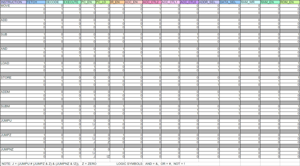
Figure 51 : micro_instructions
From this truth table the following Boolean equations can be derived (expressed in CUPL syntax) :
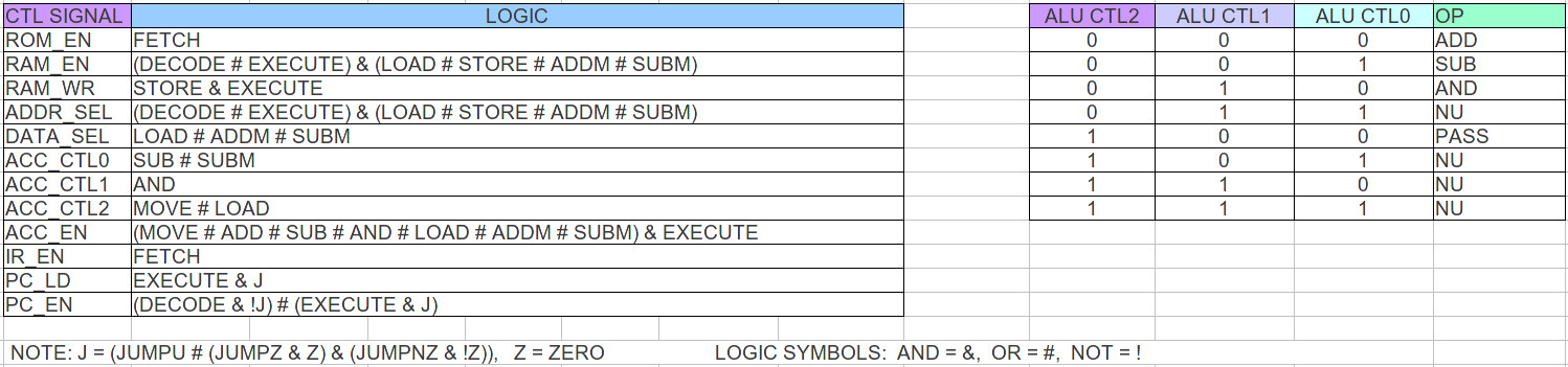
Figure 52 : control logic
The implementation of these equations, component CONTROL_LOGIC is shown in figure 53. Looking back at the previous version do confess did not implement logic as exactly defined in the control logic table, but it was functionally equivalent.
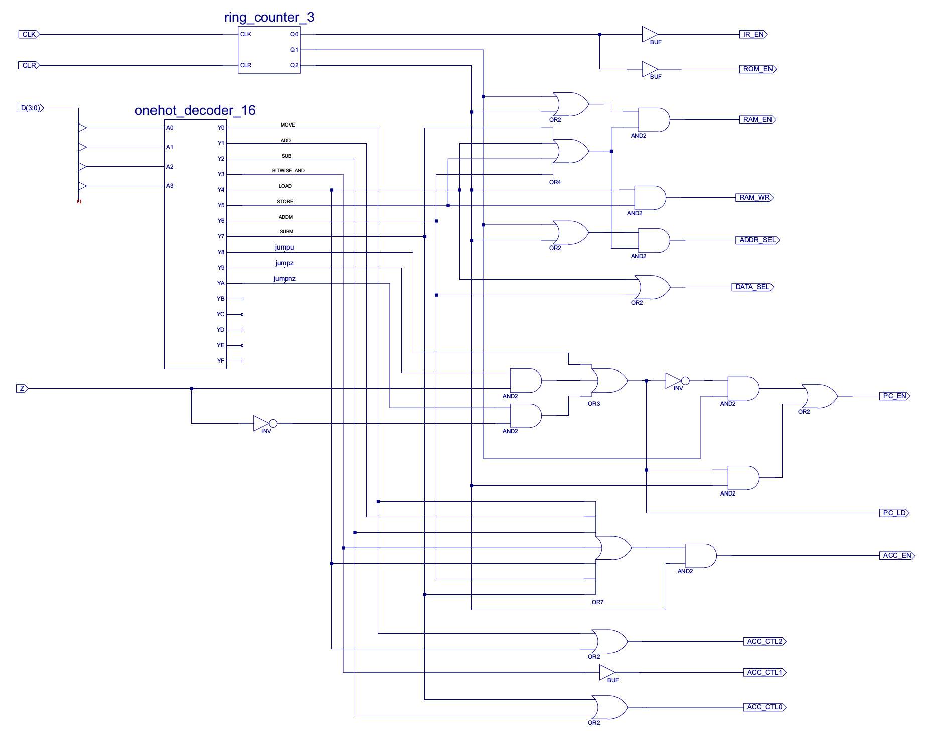
Figure 53 : Control logic decoder circuit diagram
The new and improved ISE project files for this computer can be downloaded here: (Link), version SimpleCPU_v1a1.
A small rename and cleanup. From the original simpeCPU version 1 the names of some of the hardwired controller's outputs were not quite correct, specifically ACC_CTL(2:0). These signals don't directly control the accumulator (ACC), rather they control the ALU, whos result is then stored in the ACC. Therefore, i decided to rename these signals from ACC_CTL(2:0) to ALU_CTL(2:0), as this name is more appropriate, well i guess that should simply be this name is the correct name :).
The new and improved ISE project files for this computer can be downloaded here: (Link), version SimpleCPU_v1a2. Some small changes to how the GPIO is implemented, but nothing major, the relevant schematics are shown in figures 54 - 57 below.
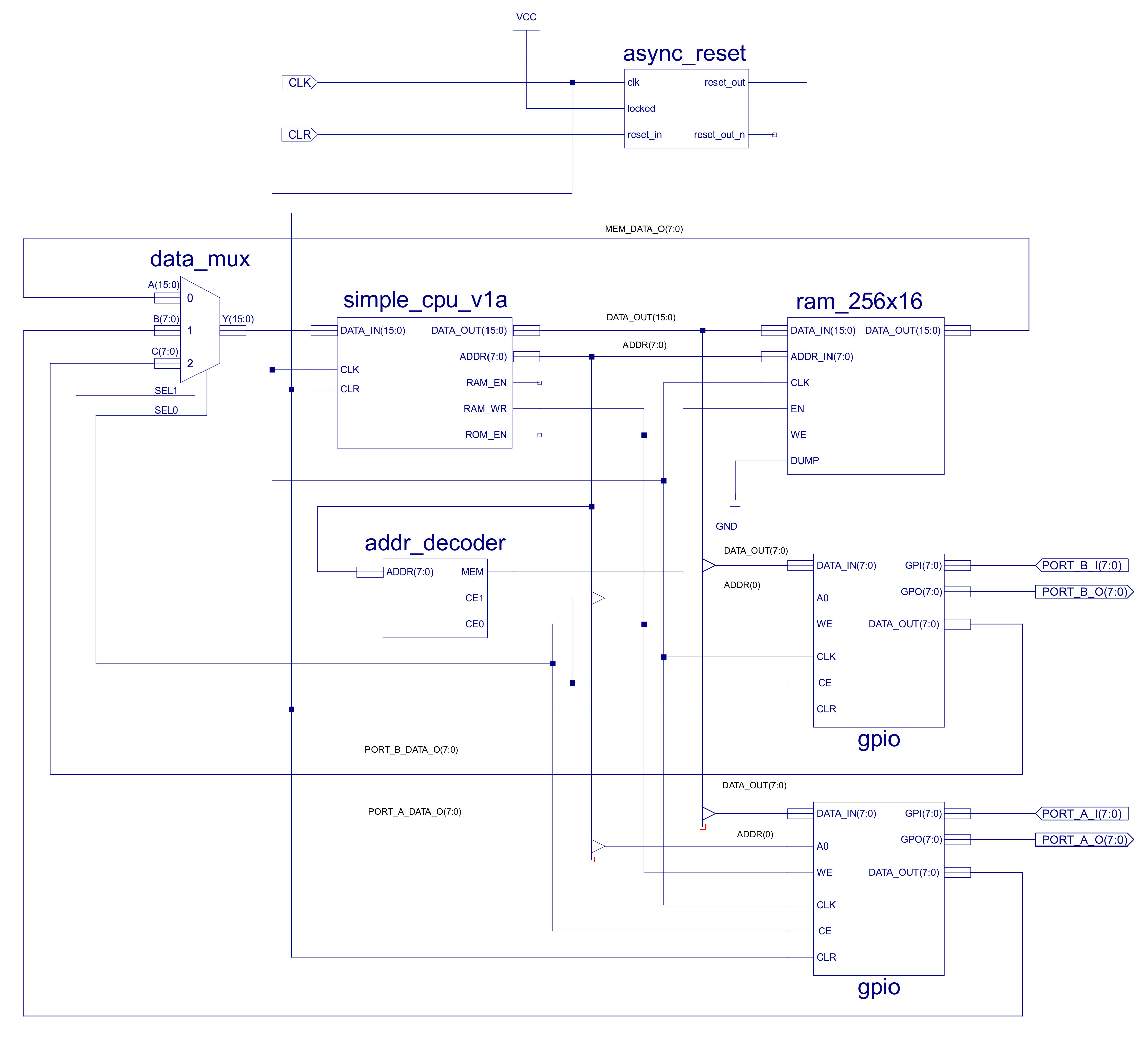
Figure 54 : new top level computer schematic
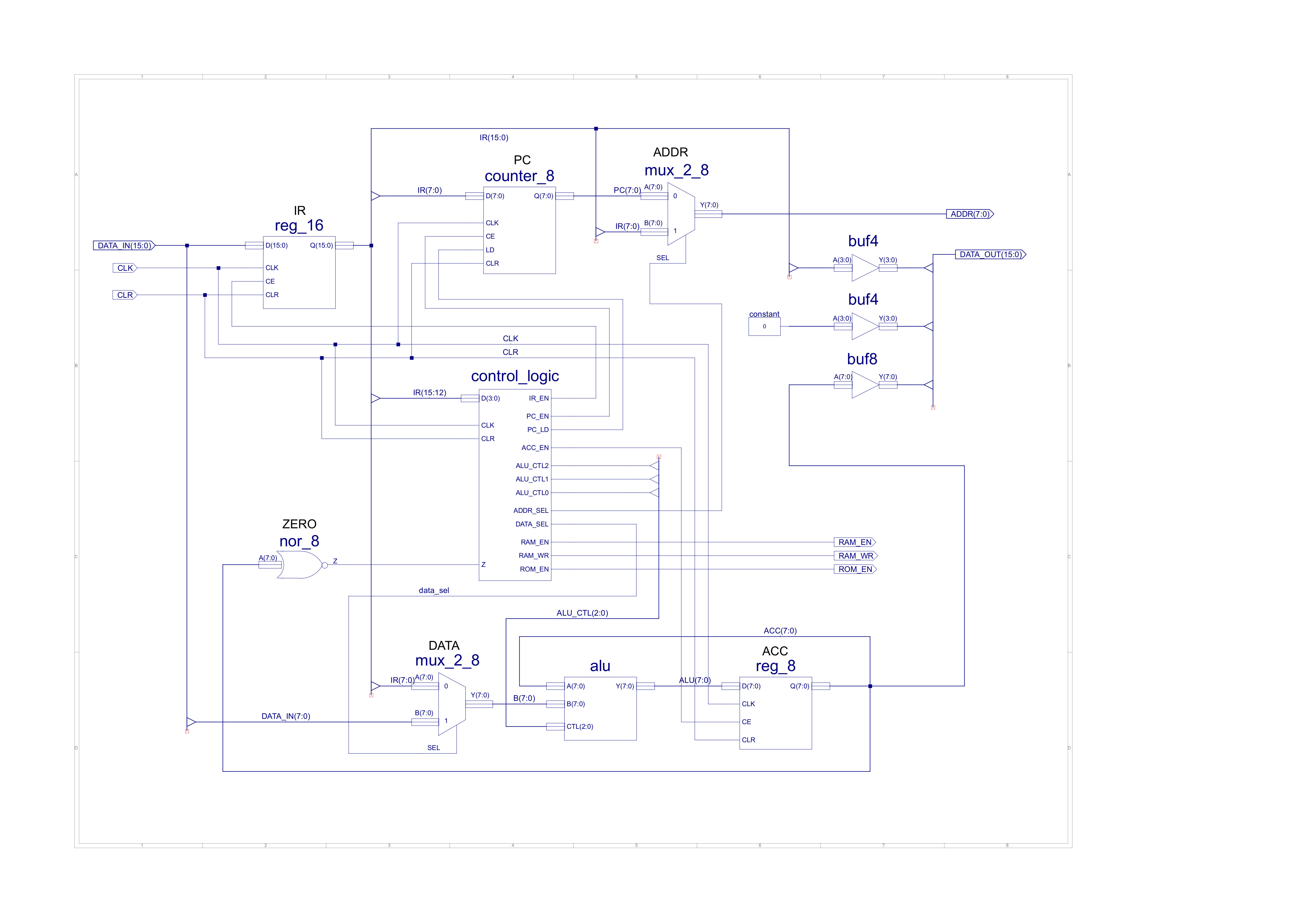
Figure 55 : new simpleCPUv1a (updated control bus)
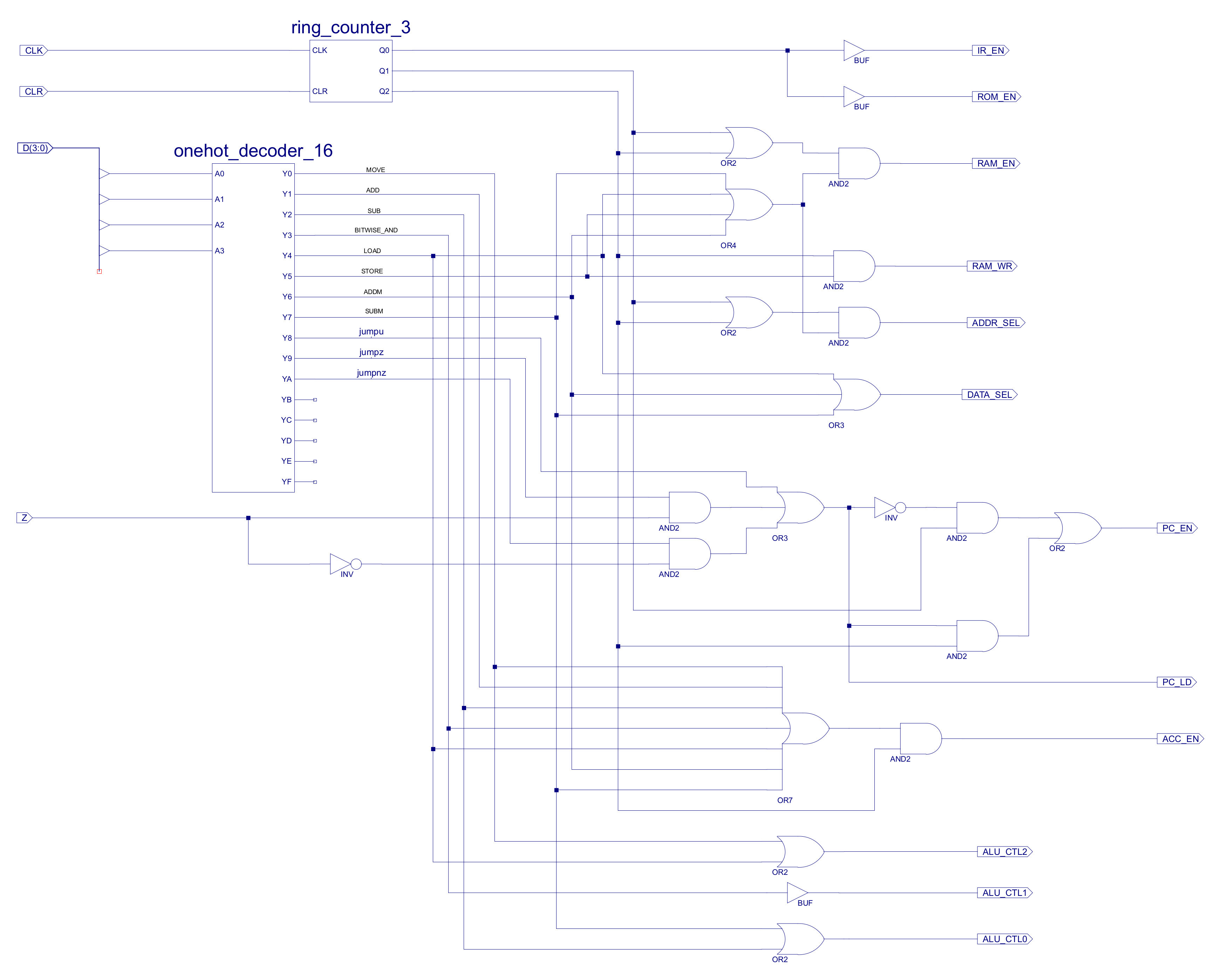
Figure 56 : new simpleCPUv1a hardwired controller
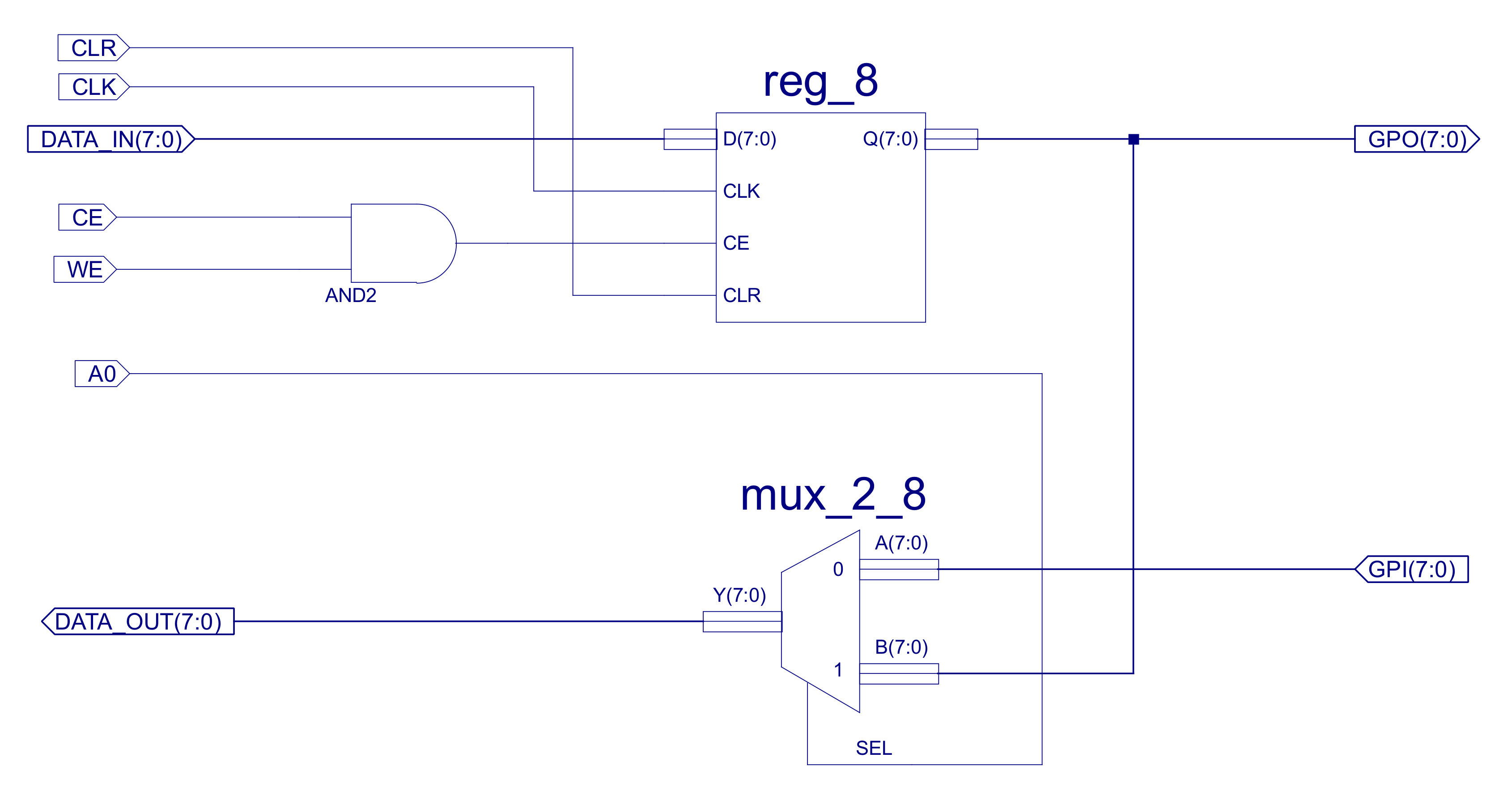
Figure 57 : new GPIO interface.
WORK IN PROGRESS

This work is licensed under a Creative Commons Attribution-NonCommercial-NoDerivatives 4.0 International License.
Contact email: mike@simplecpudesign.com