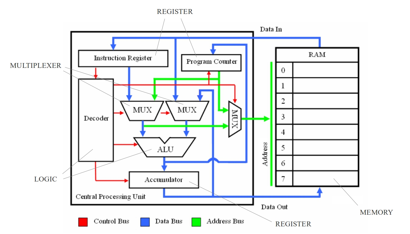
The first version of this processor (LINK) falls into the RISCy end of the CPU spectrum. To contrast the design approach taken with the original SimpleCPU I wanted to take the same basic architecture and instruction set shown in figure 1 and move it more toward the CISCy end. Therefore, at the heart of this new processor is a micro-programmed controller. Gone are the logic gates that implemented the instruction decoder, replaced with micro-instructions stored in a ROM. The aim of developing this new processor is to highlight some of the main hardware differences between RISC and CISC processors, hopefully demonstrating how simple it is to add new instructions to a micro-programmed controller, compared to a hardwired controller of the RISCy SimpleCPU. The final aim of this project is to design a computing system based on this processor which will be used in labs, such that it can be downloaded onto a Xilinx Artix-7 FPGA and programmed in machine code to produce a LED light display e.g. an overly complex Christmas tree lights controller :).
Figure 1: Top level architecture
You can trace back the ideas of the micro-programmed controller to EDSAC 2, designed by Maurice Wilkes and David Wheeler in 1958. An interesting paper on this machine can be found here (LINK). At the heart of this computer are micro-instructions stored in ROM. Originally this ROM was made out of a magnetic memory technology, these differed from your classical magnetic core memory (LINK), being more of a "transformer" based memory, an extract from the above paper is given below. This description is a little technical, ive included its as it is a very nice example of the processes involved and the hardware decisions made in designing a CPU, and the construction of a micro-programmed controller:
"The micro-programmed control was the most strikingly original feature of EDSAC 2, and demonstrated beyond doubt the practicability of this way of building the control unit of the major machine. However, it was something of a tour de force to implement a sufficiently fast read-only memory for the micro-program based on vacuum tubes. This was because none of the storage elements available for use in a read-only memory - namely diodes, capacitors and magnetic cores were well matched to the high output impedance of a vacuum tube. Later, the coming of transistors was to transform the problem and make micro-programming much more attractive from both the technical and the economic points of view. After evaluating the various alternatives, we decided to use magnetic cores for the micro-program memory. The cores were arranged in the form of a matrix and switched on the coincident current principle. The matrix contained 1024 cores and each correspond to a micro-operation in the micro-program. The cores used were 8mm in diameter. Each carried two drive winding of 40 turns each, and a bias winding of 28 turns through which a steady current was passed. The matrix was driven by a powerful vacuum tubes capable of passing a current 150mA through the drive winding. In the case of the selected core, the combined effect of the current passing through the two drive windings was sufficient to overcome the effect of the steady current passing through the bias winding and to reverse the direction of magnetisation in the core. There were about 80 sets of gates in the various parts of the machine that were controlled by the mico-program. Corresponding to each set of gates was a wire which will be referred to as the gate wire. In a particular set of gates needed to be operated when a certain micro-instruction was executed the corresponding gate wire was threaded (three times) through the core corresponding to that micro-instructions. When the core was switched an electromotive force of about 9V was induced in the wire and this was sufficient without voltage amplification to drive the gates and so cause the micro-instruction to be executed. In addition to the gate wire a further set of wires were threaded through the cores and their outputs used to determine the next core to be switched"
I like this discussion for two reasons, firstly it shows the link between hardware and architectures, a computer's final architecture is directly determined by the hardware choices of the the time i.e. what was practical to implement, performance or cost limitations. To understand why a computer looks the way it does you need to take that step back and consider all the elements / decisions that went into its construction. Secondly, even though this discussion is very much based in the past, using technologies that are no longer used, the key architectural elements discussed are still present today. Hardware has changed significantly over time, but the architectural ideas used in this machines are still relevant today when you are considering the "best" way to design a processor.
The micro-programmed controller used in this new version of the SimpleCPU processor is based on Wilke's design used in EDSAC 2, a simplified explanation of its operations is shown in figure 2. The current machine-instruction is stored in the instruction register (IR). This is decoded i.e. the opcode field is converted into the address of the first micro-instruction within the micro-programmed ROM. This translation is either done in logic or memory e.g. a look-up-table (LUT), this start address is loaded into the Control Memory Address Register (CMAR), holding the address of the first micro-instruction. A micro-instruction defines the state of the control signals and the address of the next micro-instruction. In the original design the CMAR drives a one-hot decoder, selecting one row, energising connected diode junctions in this example, rather than magnetic cores as it simplifies discussion (diode based ROM). Diodes connected to this energised row are forward biased, generating control signals and the next micro-instruction address. Note, as discussed in the above EDSAC quote these control signals may be used to directly control logic circuits e.g. bus multiplexers, or may be modified by logic gates to control other logic circuits e.g. conditional control signals. The next address contained within the accessed micro-instruction is then used to update the CMAR, allowing a series of micro-instructions to be performed over a number of clock cycles. The CMAR is therefore used as a micro-program counter, accessing a series of micro-instructions from the micro-programmed ROM i.e. the next set of control signals needed for that phase of an instructions execution. This control unit may also need to respond to external conditions e.g. carry or zero flags. This is implemented using switching nodes which control the selection of the next micro-instruction address i.e. implements a conditional jump micro-instruction, changing the value of the next micro-instruction address. This is a key difference when compared to the original SimpleCPU. The execution phase of the instruction in the original SimpleCPU was limited to one clock cycle, as the opcode field directly controls the control signals within the processor i.e. a hardwired controller. In a micro-programmed controller this one-to-one link is removed, now an instruction's execution phase can take any number of clock cycles i.e. any number of micro-instructions may be executed. To avoid having an opcode field the same size as the address bus of the micro-programmed ROM (which would be very sparse) a translation from opcode code to micro-program start address has to be implemented in hardware. Note, the exception to this is if you had a micro-programmed controller that only implemented simple instructions i.e. each machine-level instruction links to a single micro-instruction.
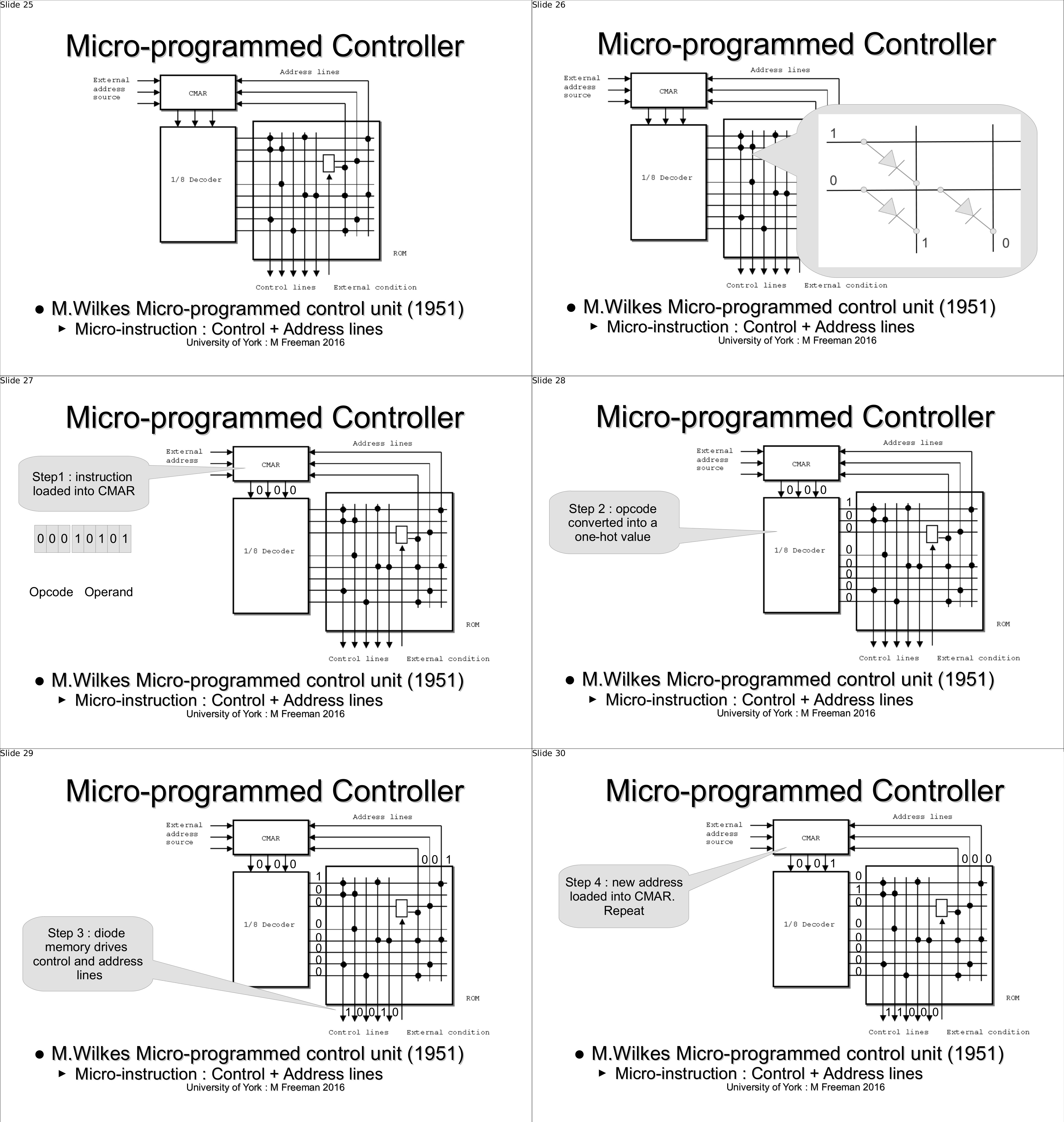
Figure 2: Micro-programmed controller operation
Unlike the previous SimpleCPU designs which used schematics, this project was written in VHDL i.e. a hardware description language. However, schematics can be automatically generated from these text files. These files were created and simulated using the Xilinx Vivado software. The file hierarchy used to define this processor and the equivalent top level schematic are shown in figure 3. Note, i named this version of the SimpleCPU processor the Minimal CISC Processor (MCP).
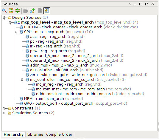
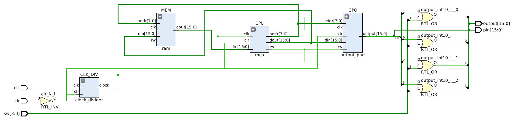
Figure 3: Top level VHDL and schematic
This system contains: CLK_DIV, CPU, RAM and GPIO. The clock divider is included to slow down the default 100MHz clock. The aim here was to simplify the delay loops used in flashing LEDs. If i remember correctly the CPU's clock speed is a blinding 6.25KHz. The processor can run a lot faster, but this just means you need more code in the software delay loops used in this application. The micro-programmed controller used within the CPU is implemented using four VHDL files:
A block diagram of the micro-programmed controller's hardware (defined in these files) is shown in figure 4. All operations within the processor are controlled by this hardware i.e. the instructions fetch, decode, execute and increment phases. To help understand the operation of this block diagram assume for the moment that an instruction has been fetched and is in the instruction register (IR), top left in figure 4. We can now consider how the 4bit opcode in this register is used to select and execute the required micro-program.
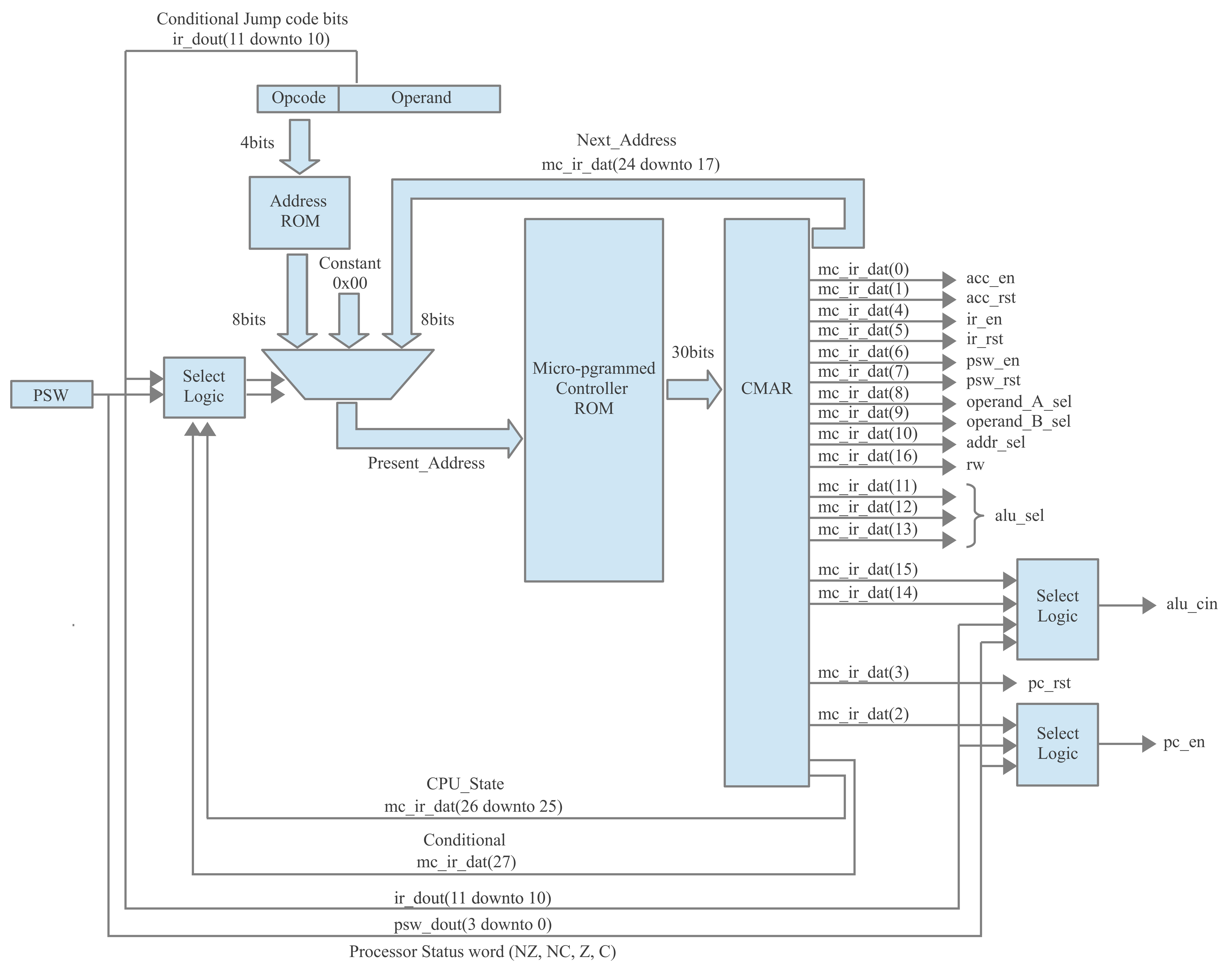
Figure 4: Micro-programmed controller block diagram
The VHDL file addr_rom.vhd performs the translation from opcode value to micro-instruction address. For the SimpleCPU processor it is assumed that the top 4bits represents the opcode. Additional bits can then be used to subdivide these instructions e.g. conditional jump instructions use a further 2bits, however, the top 4bits must be unique for each instruction type. Therefore, this memory has 16 address locations, each storing the address of the first micro-instruction of that machine-instruction. In this CPU this is an 8bit data value, as the micro-programmed ROM uses an 8bit address i.e. has 256 locations. This translation ROM could be removed if the opcode field was increased to 8bits, but this would require more instructions memory (increases instruction data width). These constants are declared in the VHDL file, as shown in figure 5. Note, the opcode value determines the location in memory e.g. the opcode for LOAD is 0000, therefore memory location 0x00 contains the address of the first micro-instruction used to implement this machine-level instruction i.e. address 0x10.
CONSTANT DATA_ROM: DATA_ROM_TABLE := DATA_ROM_TABLE'
( DATA_ROM_WORD'("00010000"), --0	Load   ACC kk : 0000 XXXX KKKKKKKK
  DATA_ROM_WORD'("00011100"), --1	And    ACC kk : 0001 XXXX KKKKKKKK
  DATA_ROM_WORD'("00000000"), --2	NU
  DATA_ROM_WORD'("00000000"), --3	NU
  DATA_ROM_WORD'("00010001"), --4	Add    ACC kk : 0100 XXXX KKKKKKKK
  DATA_ROM_WORD'("00000000"), --5	NU
  DATA_ROM_WORD'("00000000"), --6	Sub    ACC kk : 0110 XXXX KKKKKKKK
  DATA_ROM_WORD'("00000000"), --7	NU
  DATA_ROM_WORD'("00011000"), --8	Jump   U   aa : 1000 XXXX AAAAAAAA
  DATA_ROM_WORD'("00010100"), --9	Jump   ?   aa : 1001 ??XX AAAAAAAA
  DATA_ROM_WORD'("00010010"), --10	Input  ACC pp : 1010 XXXX PPPPPPPP
  DATA_ROM_WORD'("00000000"), --11	NU
  DATA_ROM_WORD'("00011001"), --12	Add    ACC pp : 1100 XXXX PPPPPPPP
  DATA_ROM_WORD'("00000000"), --13	NU
  DATA_ROM_WORD'("00010101"), --14	Output ACC pp : 1110 XXXX PPPPPPPP
  DATA_ROM_WORD'("00000000")  --15	NU
);
Figure 5: Addr_ROM.VHD - opcode to micro-instruction address translation
To illustrate how more complex instructions can be implemented in this micro-programmed controller a new machine-level instruction has been added to the instruction set:
ADD ACC pp : 1100 XXXX PPPPPPPP - ACC = ACC + M[PP]
This instruction performs a memory read and addition in a single instructions i.e. data is read from memory then added to the ACC. If this was performed on the original SimpleCPU this functionality would have to be implemented using two instructions an INPUT and a ADD. The control signals for this CPU e.g. ALU operations, MUX selection, register enable and reset, are defined in the file mc_rom.vhd, as shown in figure 6. There are 30 control signals defined for this processor, each row in the table below defines one micro-instruction i.e. the state of control signals for that phase of a machine-instructions execution. It also defines the control signal states for the instruction fetch, decode and PC counter increment phases.
-- STATE CODES             ALU_CIN
-- -----------             -------
-- 00 : FETCH              00 : 0
-- 01 : DECODE             01 : 1
-- 10 : EXECUTE            10 : not cout
-- 11 : INCREMENT          11 : cout
--
-- MICRO-INSTRUCTIONS
-- ------------------
--                      29-28 27   26-25 24-17       16 15-14   13-11   10       9        8        7       6      5      4     3      2     1       0
--                      code  cond state mc_rom_addr rw alu_cin alu_sel addr_sel op_B_sel op_A_sel psw_rst psw_en ir_rst ir_en pc_rst pc_en acc_rst acc_en
-- 00 : Fetch           00    0    00    00000001    0  00      000     0        0        0        0       0      0      1     0      0     0       0
-- 01 : Decode          00    0    01    00000000    0  00      000     0        0        0        0       0      0      0     0      0     0       0
-- 02 : Inc             00    0    11    00000000    0  01      000     0        0        1        0       0      0      0     0      1     0       0
--
-- 10 : Load   ACC kk   00    0    10    00000010    0  01      011     0        0        0        0       0      0      0     0      0     0       1
-- 11 : Add    ACC kk   00    0    10    00000010    0  00      001     0        1        0        0       1      0      0     0      0     0       1
-- 12 : Input  ACC pp   00    0    10    00010011    0  00      000     1        0        0        0       0      0      0     0      0     0       0
-- 13                   00    0    10    00000010    0  00      000     1        0        0        0       0      0      0     0      0     0       1
-- 14 : Jump   XX  aa   00    1    10    00000010    0  01      011     0        0        0        0       0      0      0     0      0     0       0
-- 15 : Output ACC pp   00    0    10    00010110    0  00      000     1        0        0        0       0      0      0     0      0     0       0
-- 16                   00    0    10    00010111    1  00      000     1        0        0        0       0      0      0     0      0     0       0
-- 17                   00    0    10    00000010    0  00      000     1        0        0        0       0      0      0     0      0     0       0
-- 18 : Jump    U  aa   00    0    10    00000000    0  01      011     0        0        0        0       0      0      0     0      1     0       0
-- 19 : Add    ACC pp   00    0    10    00011010    0  00      000     1        0        0        0       0      0      0     0      0     0       0
-- 1A                   00    0    10    00011011    0  00      000     1        0        0        0       0      0      1     0      0     0       0
-- 1B                   00    0    10    00000010    0  00      001     0        1        0        0       0      0      0     0      0     0       1
-- 1C : And    ACC kk   00    0    10    00000010    0  00      110     0        1        0        0       1      0      0     0      0     0       1
--
--   alu_sel   alu
-- s2  s1  s0  cin  InputA InputB OutputF    Function
-- 0   0   0   0      A      0     F=A       Transfer B
-- 0   0   0   1      A      0     F=A+1     Increment A
-- 0   0   1   0      A      B     F=A+B     Add B to A
-- 0   0   1   1      A      B     F=A+B+1   Add B to A + 1
-- 0   1   0   0      A  NOT B     F=A-B+1   Add 1's Comp.
-- 0   1   0   1      A  NOT B     F=A-B     Sub. B from A
-- 0   1   1   0      A      1     F=A-1     Decrement A
-- 0   1   1   1      A      1     F=A       Transfer A
-- 1   0   0   X      A      B     F=AorB    OR
-- 1   0   1   X      A      B     F=AxorB   XOR
-- 1   1   0   X      A      B     F=AandB   AND
-- 1   1   1   X      A      B     F=notA    NOT
Figure 6: MC_ROM.VHD - machine instruction control signal declarations
A summary of the various control signals is given below:
The VHDL file mc_controller.vhd is the micro-programmed controller's top level file, linking together the two ROMs, address register, multiplexers and various buffers and glue logic. The key parts of this VHDL file are shown in figure 7, these components can be matched back to the block diagram in figure 4 and the auto generated schematic in figure 8.
  -- INSTRUCTIONS
  -- ------------
  -- Load   ACC kk : 0000 XXXX KKKKKKKK
  -- And    ACC kk : 0001 XXXX KKKKKKKK
  -- Add    ACC kk : 0100 XXXX KKKKKKKK
  -- Add    ACC pp : 1100 XXXX PPPPPPPP
  -- Input  ACC pp : 1010 XXXX PPPPPPPP
  -- Output ACC pp : 1110 XXXX PPPPPPPP
  -- Jump   U   aa : 1000 XXXX AAAAAAAA
  -- Jump   Z   aa : 1001 00XX AAAAAAAA
  -- Jump   C   aa : 1001 10XX AAAAAAAA
  -- Jump  NZ   aa : 1001 01XX AAAAAAAA
  -- Jump  NC   aa : 1001 11XX AAAAAAAA

  --OPCODE drives translation ROM address bus
  addr_rom_addr <= ir_dout( 15 DOWNTO 12 );

  acc_en        <=  mc_ir_dat(0);
  acc_rst       <=  mc_ir_dat(1);

  -- PSW REGISTER
  -- ------------
  -- BIT0 = Carry
  -- BIT1 = Zero
  -- BIT2 = not Carry
  -- BIT3 = not Zero

  -- mc_ir_dat(2) = pc_en
  -- mc_ir_dat(27) = condition instructions, enable PC is status true

  pc_en         <=  mc_ir_dat(2) WHEN mc_ir_dat(27)='0' ELSE
                    '1'          WHEN ir_dout( 11 DOWNTO 10 )="11" and psw_dout_int(2)='1' ELSE
                    '1'          WHEN ir_dout( 11 DOWNTO 10 )="01" and psw_dout_int(3)='1' ELSE
                    '1'          WHEN ir_dout( 11 DOWNTO 10 )="10" and psw_dout_int(0)='1' ELSE
                    '1'          WHEN ir_dout( 11 DOWNTO 10 )="00" and psw_dout_int(1)='1' ELSE
                    '0';

  pc_rst        <=  mc_ir_dat(3);
  ir_en         <=  mc_ir_dat(4);
  ir_rst        <=  mc_ir_dat(5);
  psw_en        <=  mc_ir_dat(6);
  psw_rst       <=  mc_ir_dat(7);
  operand_A_sel <=  mc_ir_dat(8);
  operand_B_sel <=  mc_ir_dat(9);
  addr_sel      <=  mc_ir_dat(10);

  alu_sel       <=  mc_ir_dat(13 DOWNTO 11);

  -- mc_ir_dat(15 DOWNTO 14) = alu_cin select: 0 or 1

  alu_cin       <= '0'             WHEN mc_ir_dat(15 DOWNTO 14)="00" ELSE
                   '1'             WHEN mc_ir_dat(15 DOWNTO 14)="01" ELSE
                   not psw_dout(0) WHEN mc_ir_dat(15 DOWNTO 14)="10" ELSE
                   psw_dout(0);

  rw            <= not mc_ir_dat(16);

  -- mc_ir_dat(26 DOWNTO 25) = processor state
  -- 00 = Fetch
  -- 01 = Decode
  -- 10 = Execute
  -- 11 = Increment

  -- addr_rom_data = address of first micro instruction
  -- 00000000 = address of fetch micro instruction
  -- mc_ir_dat( 24 DOWNTO 17 ) = address of next micro instruction

  mc_rom_addr   <= addr_rom_data WHEN mc_ir_dat(26 DOWNTO 25)="01" ELSE
                   "00000000"    WHEN mc_ir_dat(27)='1' and ir_dout( 11 DOWNTO 10 )="11" and psw_dout_int(2)='1' ELSE
                   "00000000"    WHEN mc_ir_dat(27)='1' and ir_dout( 11 DOWNTO 10 )="01" and psw_dout_int(3)='1' ELSE
                   "00000000"    WHEN mc_ir_dat(27)='1' and ir_dout( 11 DOWNTO 10 )="10" and psw_dout_int(0)='1' ELSE
		   "00000000"    WHEN mc_ir_dat(27)='1' and ir_dout( 11 DOWNTO 10 )="00" and psw_dout_int(1)='1' ELSE
                   mc_ir_dat( 24 DOWNTO 17 );

  psw_dout_int  <= psw_dout; --"00000000" WHEN mc_ir_dat(26 DOWNTO 25)="00" ELSE psw_dout;

  --
  -- COMPONENTS
  --

  -- micro-programmed ROM address register (CMAR)
  mc_ir_reg : reg
  GENERIC MAP(
    width => 30 )
  PORT MAP(
    clk  => clk,
    clr  => clr,
    en   => VCC,
    rst  => GND,
    din  => mc_rom_data,
    dout => mc_ir_dat );

  -- micro-programmed ROM
  mc_rom_inst : mc_rom
  GENERIC MAP(
    SIMULATION => TRUE,
    ADDR_WIDTH => 8,
    DATA_WIDTH => 30 )
  PORT MAP(
    addr => mc_rom_addr,
    data => mc_rom_data );

  -- micro-instruction address look up table
  addr_rom_inst : addr_rom
  GENERIC MAP(
    SIMULATION => TRUE,
    ADDR_WIDTH => 4,
    DATA_WIDTH => 8 )
  PORT MAP(
    addr => addr_rom_addr,
    data => addr_rom_data );
Figure 7: key sections of mc_controller.vhd
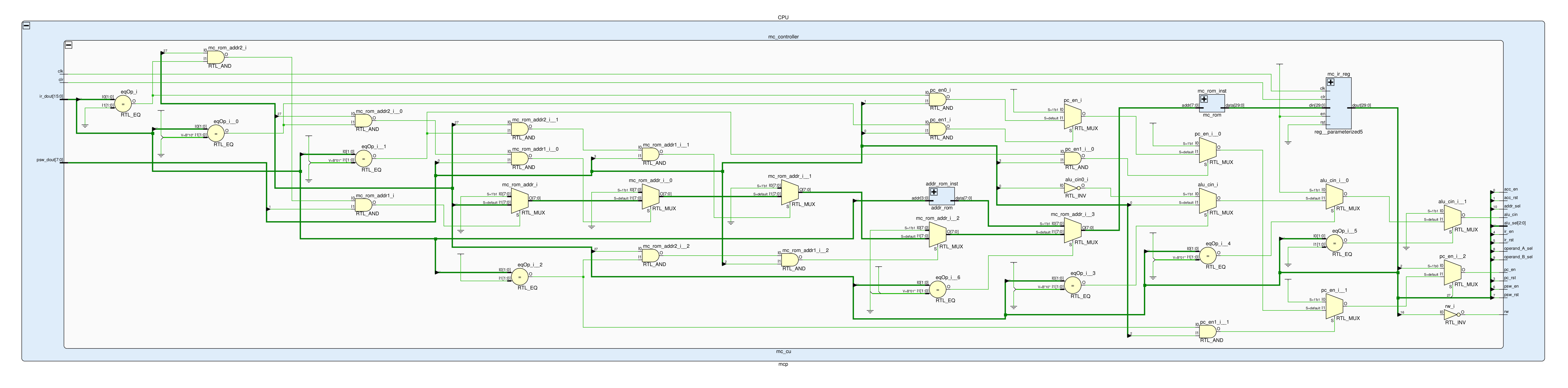
Figure 8: micro-programmed control circuit diagram
Most of the control signals stored in the micro-programmed ROM are connected directly to the various hardware components in the processor e.g. registers and multiplexers. There are three control signals that can be modified by the processor's state i.e. the Processor's Status Word (PSW) or instruction phase (fetch, decode, execute or increment), these signals are:
The VHDL used to select the micro-programmed ROM's next address:mc_rom_addr and its equivalent pseudo code is shown below. This logic selects the output of the address ROM addr_rom if the CPU is in the decode phase. If the machine-instruction is a conditional jump and that condition is true, the address is set to the micro-instruction that performs an instruction fetch i.e. address 0, skipping the PC increment phase. The PC is loaded with the jump address defined in the IR by the pc_en logic. Otherwise the next address is taken from the micro-programmed ROM e.g. if an machine-level instruction is made up of multiple micro-instructions.
VHDL
----
mc_rom_addr   <= addr_rom_data WHEN mc_ir_dat(26 DOWNTO 25)="01" ELSE
                 "00000000"    WHEN mc_ir_dat(27)='1' and ir_dout( 11 DOWNTO 10 )="11" and psw_dout_int(2)='1' ELSE
                 "00000000"    WHEN mc_ir_dat(27)='1' and ir_dout( 11 DOWNTO 10 )="01" and psw_dout_int(3)='1' ELSE
                 "00000000"    WHEN mc_ir_dat(27)='1' and ir_dout( 11 DOWNTO 10 )="10" and psw_dout_int(0)='1' ELSE
	         "00000000"    WHEN mc_ir_dat(27)='1' and ir_dout( 11 DOWNTO 10 )="00" and psw_dout_int(1)='1' ELSE
                 mc_ir_dat( 24 DOWNTO 17 );

PSEUDO CODE
-----------
IF CPU_STATE = DECODE
THEN
   ADDRESS = ADDRESS OF FIRST MICRO-INSTRUCTION          -- data stored in address ROM
ELSE
   IF CONDITIONAL INSTRUCTION = TRUE                     -- is machine-level instruction a conditional jump?
   THEN
      IF ((INSTRUCTION = JUMP NC) AND (PSW = NC)) OR
         ((INSTRUCTION = JUMP NZ) AND (PSW = NZ)) OR
         ((INSTRUCTION = JUMP Z) AND (PSW = Z)) OR
         ((INSTRUCTION = JUMP C) AND (PSW = C))
      THEN
         ADDRESS = 0
      END IF
   ELSE
      ADDRESS = ADDRESS STORED IN MICRO-PROGRAMMED ROM   -- next address defined in current micro-instruction
   END IF
END IF
The VHDL used to implement the program counter enable signal:pc_en and its equivalent pseudo code is shown below. This logic selects the value stored in the micro-programmed ROM if the instruction is not conditional. This value is normally zero, except for the increment PC micro-instruction (address 0x02, final phase/state of an instruction) and the unconditional JUMP instruction (address 0x18). If it is a conditional instruction the PSW register bits are checked, if true the PC is updated. As the ALU is set as pass-through and the multiplexers are set to their default values, the IR operand field is passed through to the PC input i.e. the jump address. Again, if the unconditional JUMP is taken the increment phase is skipped and the next instruction fetched.
VHDL
----
pc_en         <=  mc_ir_dat(2) WHEN mc_ir_dat(27)='0' ELSE
                  '1'          WHEN ir_dout( 11 DOWNTO 10 )="11" and psw_dout_int(2)='1' ELSE
                  '1'          WHEN ir_dout( 11 DOWNTO 10 )="01" and psw_dout_int(3)='1' ELSE
                  '1'          WHEN ir_dout( 11 DOWNTO 10 )="10" and psw_dout_int(0)='1' ELSE
                  '1'          WHEN ir_dout( 11 DOWNTO 10 )="00" and psw_dout_int(1)='1' ELSE
                  '0';
PSEUDO CODE
-----------
IF CONDITIONAL INSTRUCTION = FALSE
THEN
   PC_ENABLE = VALUE STORED IN MICRO-PROGRAMMED ROM
ELSE
   IF ((INSTRUCTION = JUMP NC) AND (PSW = NC)) OR
      ((INSTRUCTION = JUMP NZ) AND (PSW = NZ)) OR
      ((INSTRUCTION = JUMP Z) AND (PSW = Z)) OR
      ((INSTRUCTION = JUMP C) AND (PSW = C))
   THEN
      PC_ENABLE = TRUE
   ELSE
      PC_ENABLE = FALSE
   END IF
END IF
The VHDL used to implement the alu carry in signal:alu_cin and its equivalent pseudo code is shown below. This logic selects either a hard coded value or the previous carry bit stored in the processor's status register. The hard-coded constants are used to control the increment and decrement functions within the alu. Otherwise the previous state of the carry bit is used to enable arithmetic functions that are larger than eight bits.
VHDL
----
alu_cin       <= '0'             WHEN mc_ir_dat(15 DOWNTO 14)="00" ELSE
                 '1'             WHEN mc_ir_dat(15 DOWNTO 14)="01" ELSE
                 not psw_dout(0) WHEN mc_ir_dat(15 DOWNTO 14)="10" ELSE
                 psw_dout(0);
PSEUDO CODE
-----------
IF VALUE STORED IN MICRO-PROGRAMMED ROM = SET TO ZERO
THEN
   ALU_CARRY_IN = 0
ELSE
   IF VALUE STORED IN MICRO-PROGRAMMED ROM = SET TO ONE
   THEN
      ALU_CARRY_IN = 1
   ELSE
      IF VALUE STORED IN MICRO-PROGRAMMED ROM = SET TO NOT C
      THEN
         ALU_CARRY_IN = NOT (PROCESSOR STATUS WORD BIT 0)
      ELSE
         IF VALUE STORED IN MICRO-PROGRAMMED ROM = SET TO NOT C
         THEN
            ALU_CARRY_IN = PROCESSOR STATUS WORD BIT 0
         END IF
      END IF
   END IF
END IF
As this new processor (MCP) implements the same simple instruction set as the original SimpleCPU the majority of the machine-level instructions map to a single micro-instruction, as they were/are executed over a single cycle. As previously discussed to show the power :) of a CISCy instruction consider the new ADD instruction added:
ADD ACC pp : 1100 XXXX PPPPPPPP - ACC = ACC + M[PP]
This instruction combines together the INPUT and a ADD micro-instructions as shown below. The first micro-instruction drives the specified address in the IR onto the main memory address bus. On the next clock cycle the next micro-instruction captures this data in the IR i.e. the IR is re-purposed/used as a temporary data buffer. Finally, the last micro-instruction adds the lower 8bits of the IR (containing the data) to the ACC. As with all non-jump instructions the micro-programmed control then goes to the increment PC micro-instruction at address 0x02 (within the micro-programmed ROM).
-- MICRO-INSTRUCTIONS
-- ------------------
--                      29-28 27   26-25 24-17       16 15-14   13-11   10       9        8        7       6      5      4     3      2     1       0
--                      code  cond state mc_rom_addr rw alu_cin alu_sel addr_sel op_B_sel op_A_sel psw_rst psw_en ir_rst ir_en pc_rst pc_en acc_rst acc_en
-- 19 : Add    ACC pp   00    0    10    00011010    0  00      000     1        0        0        0       0      0      0     0      0     0       0
-- 1A                   00    0    10    00011011    0  00      000     1        0        0        0       0      0      1     0      0     0       0
-- 1B                   00    0    10    00000010    0  00      001     0        1        0        0       0      0      0     0      0     0       1
The main benefit of a micro-programmed controller is that once you have one up and running its relatively simple to add new instructions. To illustrate this we can add an immediate XOR instruction:
XOR ACC kk : 0010 XXXX KKKKKKKK - ACC = ACC xor KK
The opcode is selected from the list of free memory locations in the address ROM addr_rom.vhd: 2,3,5,7,11,13 and 15, in this case went for opcode 0x2, but any free value would do. At this address the address of the next free micro-instruction (address) in the micro-programmed ROM is stored, in this case 0x1D.
DATA_ROM_WORD'("00011101"), --2 XOR ACC kk : 0010 XXXX KKKKKKKK
The XOR instruction is basically the same as the AND instruction the only thing that needs to be changed in the new micro-instruction is the alu_sel lines, configuring the ALU to perform a XOR function (101) rather than an AND function (110), as shown below. Note, the ALU function codes are shown in figure 6.
-- MICRO-INSTRUCTIONS
-- ------------------
--                      29-28 27   26-25 24-17       16 15-14   13-11   10       9        8        7       6      5      4     3      2     1       0
--                      code  cond state mc_rom_addr rw alu_cin alu_sel addr_sel op_B_sel op_A_sel psw_rst psw_en ir_rst ir_en pc_rst pc_en acc_rst acc_en
-- 1D : Xor    ACC kk   00    0    10    00000010    0  00      101     0        1        0        0       1      0      0     0      0     0       1
If a new instruction was to be added to the original SimpleCPU a new hardwired controller would need to be designed i.e. logic gates would need to be added to drive the correct value onto the alu_sel lines. This isn't overly complex, but it is significantly more work than changing a few bits within a ROM file. The other benefit is that the processor's hardware components i.e. its hardware architecture, is not changed. Therefore, the processor's critical path delay is not altered, making it less likely that timing errors will be introduced. The micro-programmed control is integrated with the other hardware components used in the original SimpleCPU. The auto generated schematic of this circuit is shown in figure 9, again you can match component blocks back to the original block diagram shown in figure 1.
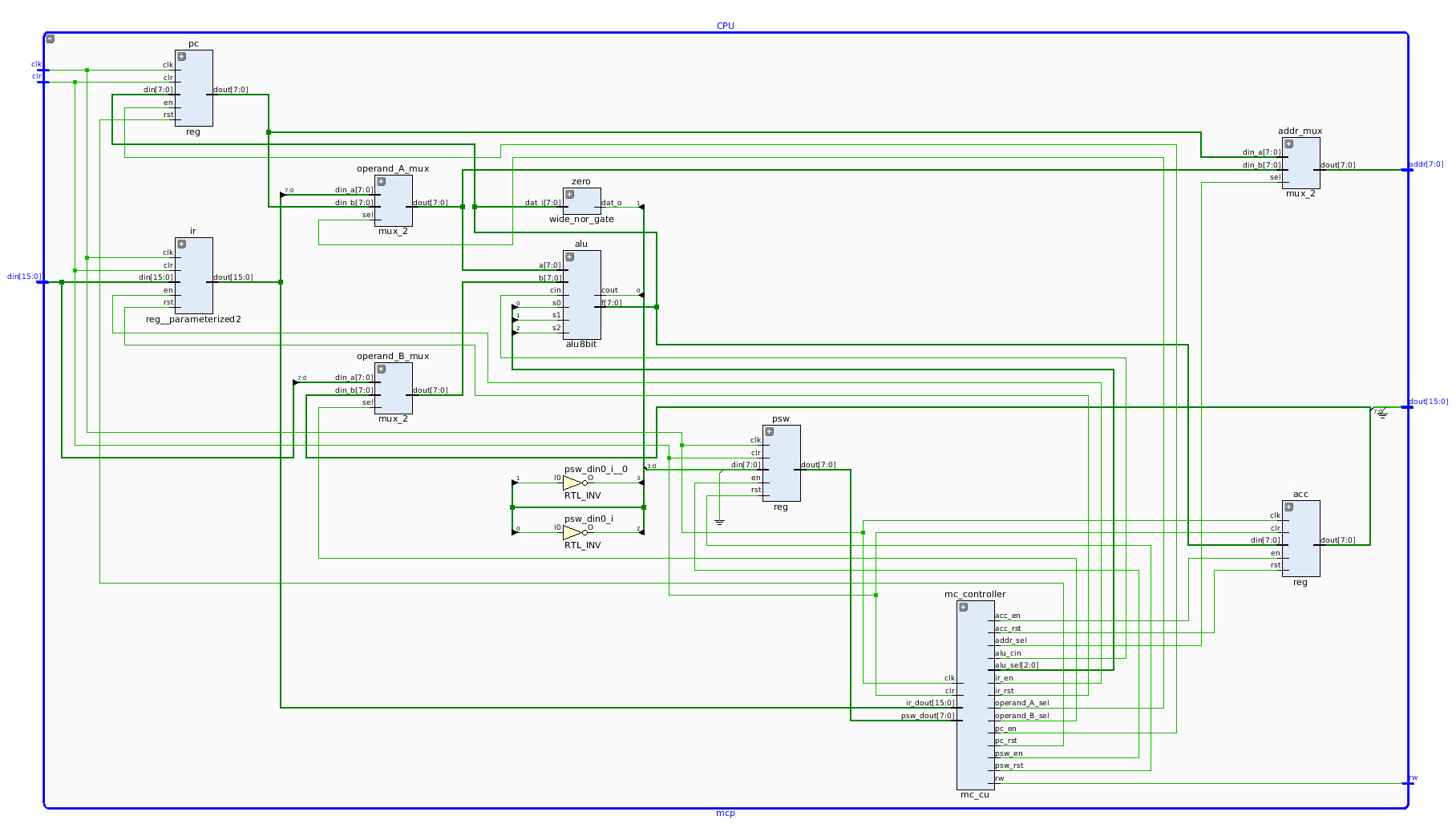
Figure 9: MCP processor
Figure 10: Top level schematic
This system contains: CLK_DIV, CPU, RAM and GPIO. The 16 general purpose outputs are connected to LEDs. Driving a logic '1' onto an output pin will cause the associated LED to be illuminated. In addition to these outputs there are also four inputs (sw). These are not connected to the processor, but are logically ORed with output port bits 0,1,2 and 3 (shown in figure 10). This allows you to test if the FPGA has been configured correctly i.e. if one of these switches is moved into the logic '1' position an LED will be illuminated. The mapping between output pins and LEDs is define in a Vivado configuration file shown in figure 11.
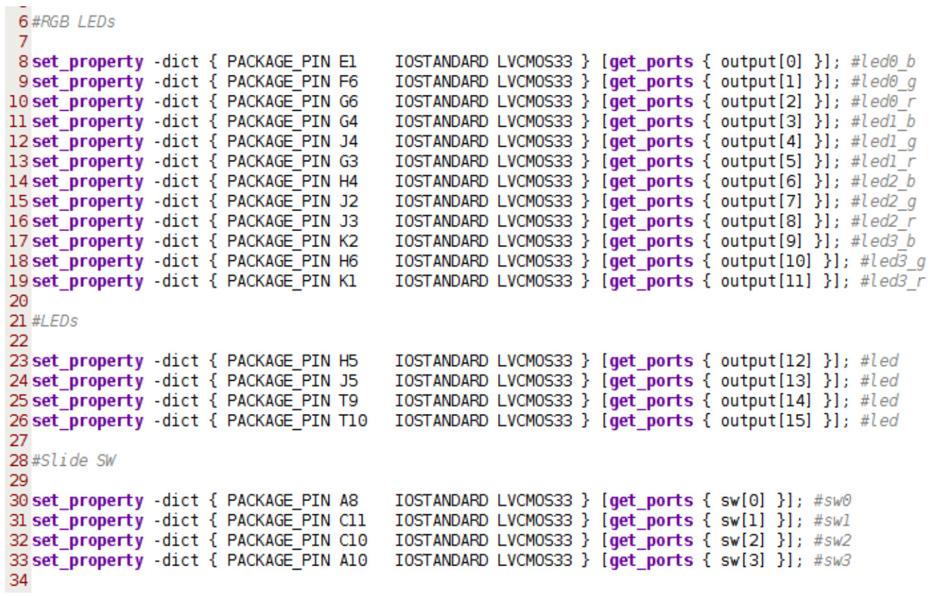
Figure 11: FPGA pin connections
To enter a program for this processor the VHDL file ram.vhd is edited i.e. the raw machine code. Like all VHDL components this file contains two main sections: Entity and Architecture, shown in figure 12. The Entity section defines this hardware component's interface (ports) i.e. the physical pins that are need on the actual hardware device:
Note, for some memory technologies the data bus is a single, bi-directional bus. This reduces the number of physical pins needed on the device, as the same pins are used as both inputs and outputs (multiplexed), but this does complicate its operations i.e. you need to connect and disconnect different drivers when performing reads or writes, as a result there is a turn-over (turn-around) period when no driver is connected, this slows down the memories average performance. For the hardware we will be using (FPGAs) these types of bi-directional buses are not generally supported / recommended, hence we tend to have separate uni-directional data-in and data-out buses.
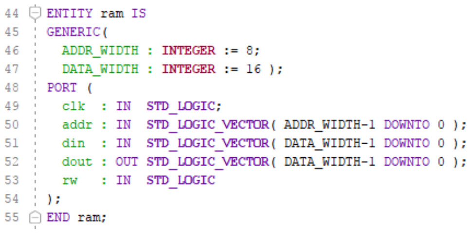
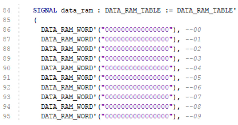
Figure 12: ram.vhd, Entity (top) and Architecture data declaration (bottom)
The VHDL components Architecture defines how the inputs and outputs are connected. The section of VHDL shown in figure 12 is the ROM data constant declarations, each line defines the data stored at that address. The processor uses a 16bit fixed length instruction, as shown in figure 1. These use a 4bit opcode, followed by an 8bit immediate value (KK), data memory address (PP) or an instruction memory address (AA). Jump instructions also contain a 2bit bit field, selecting the conditional flag used. To test if the system is working correctly the test code below was used:
INSTRUCTION         ADDR          DATA
start:
   input A           0      1010 0000 00000100
   add 01            1      0100 0000 00000001
   output A          2      1110 0000 00000100
   jump start        3      1000 0000 00000000

A: .data 2 0         4      0000 0000 00000000
This program repeatedly increments variable A (stored at address 0x04). As this code does not produce any outputs it was tested using the simulator, the waveform traces are shown below in figure 13.
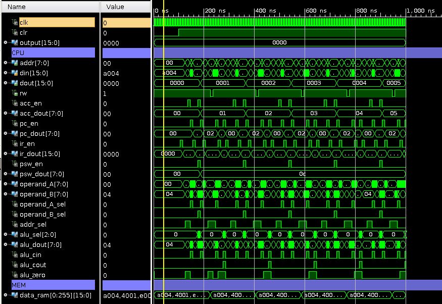
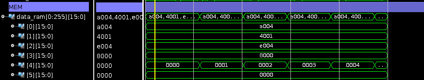
Figure 13: simulation
In addition to a memory device this processor also has a 16bit output port i.e. the processor can control the state of 16 wires, setting their individual values to either a logic '1' or a logic '0'. The hardware used to implement this functionality is memory mapped to addresses 0xFF and 0xFE i.e. its functionality is triggered when the processor writes to memory address 0xFF or 0xFE. To identify when this operation is performed by the processor the address decoder logic shown in figure 14 is used. When the address bus lines A7 – A1 are all logic '1' and the read/write (R/W) control line is a logic '0' the CE line is enabled. This is then combined with A0, enables either the low or high byte on the output port to be updated .
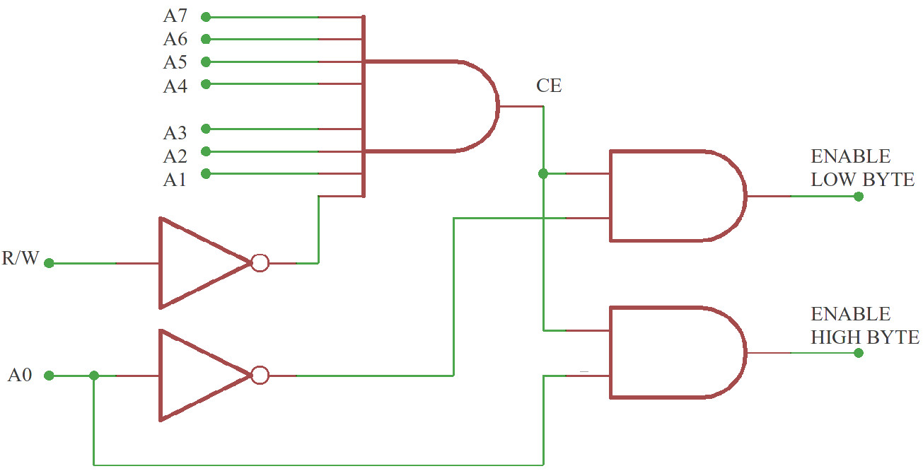
Figure 14: GPIO address decoding logic
Note, the output port is just a bank of 16 flip-flops, their D inputs are connected to the data bus (D7-D0), their Q outputs connect to external wires (LEDs). These signals can not be read by the processor i.e. their Q outputs are not connected back to the CPU's data bus. The flip-flops also have an enable line, if this is low the clock (update signal) is ignored, eight flip-flips are connect to ENABLE_LOW_BYTE, eight to ENABLE_HIGH_BYTE, as the OUTPUT instruction can only write 8bit values to memory (16bits written in two 8bit chunks).
The aim of this project is to create an LED display i.e. lots of flashing lights. To control the speed at which these LEDs (output port) are updated we will need to implement a software delay loop i.e. a piece of code that effectively wastes processor cycles, delaying the progression of the program. To minimise the size of this code a hardware clock divider is included, to slow down the default 100MHz clock, reducing the system's clock speed to 6.25KHz, a clock period of 160us. Typically an instruction takes four clock cycles, therefore, running at this frequency an instruction will normally take 0.64ms. The processor can run a lot faster, but, as the main function of the processor is to generate low frequency output sequences / patterns, and is not intended to perform "number crunching" applications a slow clock speed simplifies the implementation i.e. means you need less code in the software delay loops. The software to turn on/off an LED every 650ms is shown below:
INSTRUCTION	ADDR	DESCRIPTION		       DATA
start:
   load 0	0	ACC = 0x00		0000 0000 00000000
   output 15	1	M[0x09] = ACC		1110 0000 00001111
   input 15	2	ACC = M[0x09]		1010 0000 00001111
   add 1	3	ACC = ACC + 1		0100 0000 00000001
   jump nc 1    4      	loop until overflow 	1001 1100 00000001
   load 128     5       ACC = 0x80              0000 0000 10000000
   output 255	6	M[0xFF] = ACC		1110 0000 11111111
   load 0	7	ACC = 0x00		0000 0000 00000000
   output 15	8	M[0x09] = ACC		1110 0000 00001111
   input 15	9	ACC = M[0x09]		1010 0000 00001111
   add 1	10	ACC = ACC + 1		0100 0000 00000001
   jump nc 8    11     	loop until overflow 	1001 1100 00001000
   load 0       12      ACC = 0x00              0000 0000 00000000
   output 255	13	M[0xFF] = ACC		1110 0000 11111111
   jump 0       14      loop                    1000 0000 00000000

C: .data 2 0	15	variable COUNT		0000 0000 00000000
This delay loop should produce a delay of:
Delay = (3 + (4 x 256)) x 0.64ms = 650 ms
This VHDL source code was synthesised and download into a Xilinx Artix-7 FPGA board. A video of the LED flashing is available here: (LINK), the small green LED top left. This video also shows how the four test switches change the colour of the RGB LEDs.
An example lab script based on this hardware are available here:
At the end of the Autumn term, round about Christmas students were set the challenge to create a Christmas LED light display, controlling LEDs LD7 - LD0 onf the FPGA PCB:
A video of the finished LED display is available here: (LINK).

This work is licensed under a Creative Commons Attribution-NonCommercial-NoDerivatives 4.0 International License.
Contact email: mike@simplecpudesign.com